In the field of electronic engineering, printed circuit boards (PCBs) are indispensable components that carry the connections and communication between electronic components. PCBs are not single-layer structures, but are composed of multiple layers, each with its specific functions and roles. Let’s talk about them together.
1. Mechanical layer
Definition: The mechanical layer represents the overall appearance and size of the PCB board.
Function: It defines the boundaries, dimensions, assembly instructions, and other information related to mechanical characteristics of the circuit board.
Usage precautions: The mechanical layer is often output and displayed together with other layers, but should not be used for electrical wiring.
2. Keep Out Layer
Definition: This layer defines the areas on the PCB board that allow for wiring or placement of components.
Function: By drawing enclosed areas, boundaries are set for automatic layout and routing to ensure the effectiveness of circuit design.
Usage precautions: The wiring layer should not be confused with the mechanical layer, and its boundaries define the scope of electrical wiring.
3. Signal Layer
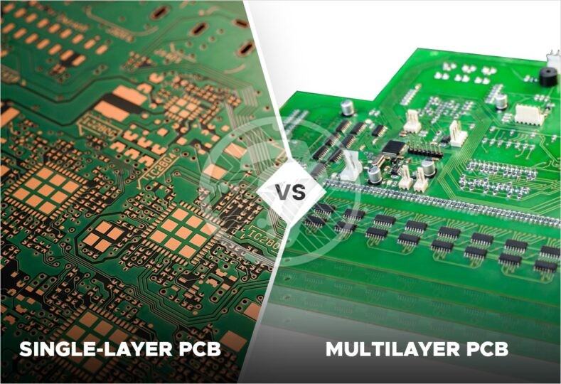
Definition: The signal layer is the area on a PCB board used for arranging wires, including the top layer, bottom layer, and middle layers.
Function: The top and bottom layers are usually used to place components, while the middle layer is used for wiring, achieving electrical connections between components.
Layer count: According to design requirements, a PCB can have multiple intermediate layers for complex wiring designs.
4. Top Paste and Bottom Paste
Definition: These two layers represent the top and bottom layers of the solder pad steel mesh.
Function: In SMT (Surface Mount Technology), the Top Paste and Bottom Paste layers are used to make steel mesh, ensuring uniform application of solder paste and optimizing the welding process.
Application: The holes on the steel mesh match the size of the solder pad, ensuring that the solder paste can be accurately applied to the solder pad.

