PCB design is an important part of the overall PCB design, which determines the foundation of the entire PCB. PCB suppliers have summarized a few points to note in PCB design, which we hope will be helpful to you.
1, select the PCB board
Selecting a PCB board must balance meeting design requirements with volume production and cost. Design requirements include both electrical components and mechanical components. This material issue is even more important when designing ultra-high speed PCBs (greater than GHz). For example, the commonly used FR-4 material, the dielectric loss at several GHz frequency has a significant impact on signal attenuation. On the electrical side, the design side needs to focus on whether the dielectric constant and dielectric loss are consistent at the same frequency.
2, avoiding high frequency interference
The basic idea of avoiding high-frequency interference is to minimize interference from the electromagnetic field of the high-frequency signal, i.e., crosstalk. You can use distance between the high speed signal and the analog signal, or add ground protection/shunt channels next to the analog signal, and be aware of interference from digital ground noise to the analog ground.
3, Addressing signal integrity issues
Signal integrity is basically a matter of impedance matching. Factors that affect impedance matching include the signal source architecture and output impedance, the characteristic impedance of the trace, the characteristics of the load side, and the topology of the trace. The solution is to terminate and adjust the topology of the trace.
4, Implementing differential wiring
There are two things to keep in mind about differential pair wiring. One is that the length of the two lines should be as long as possible, and the other is that the spacing between the two lines (determined by the differential impedance) should remain the same, i.e., remain parallel. There are two types of parallelism. One is that both lines are on the same layer, and the other is that both lines are on the upper and lower layers. Usually, the former has been implemented in more ways.
5. Execute differential distribution line with only one output clock signal line
To use differential routing, it must make sense for both the source and receiver to be differential signals. Therefore, differential routing cannot be used for clock signals that have only one output.
6. Matching resistance between differential pairs at the receiver
Usually a matching resistor is added between the differential pairs at the receiver side, and its value should be equal to the value of the differential impedance. This results in better signal quality.
7. Wiring of differential pairs should be closely parallel
Differential pairs should be wired correctly closed and parallel. The proper proximity is because that spacing affects the value of the differential impedance, which is an important parameter for designing differential pairs. Parallelism is also required because it maintains the consistency of the differential impedance. If the two lines are too close together, the differential impedance will not be consistent, which will affect signal integrity and time delay.
8, dealing with some theoretical conflicts in practical wiring
(1), basically, the isolated analog/digital partition is correct. It is important to note that the signal traces should not cross the partitioned area as much as possible, and the return current paths for power and signal should not be too large.
(2), a crystal oscillator is an analog positive feedback oscillator circuit. To obtain a stable oscillating signal, the loop gain and phase specifications must be met. The oscillation specification of the analog signal is susceptible to interference, and even if the analog signal is added, the interference cannot be completely isolated. Also the distance is too far and the noise on the plane will affect the positive feedback oscillator circuit. Therefore, the distance between the crystal and the chip must be very close.
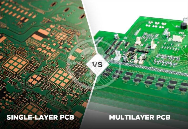
These are the issues that multilayer PCB manufacturers should be aware of when designing a circuit board. Have you learned it?

