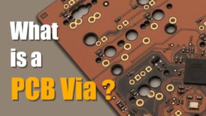
Via is an important part of multilayer boards, and drilling typically accounts for 30% to 40% of the cost of board fabrication. However, vias should be valued in PCBs not only for their quantity and price, but also for the proper vias size, quantity, distance between vias and vias and alignments, components, vias capacitance, vias inductance, and more. All can have a certain impact on the design of a good performance of the PCB. Today, we are talking about those holes on the circuit board.
Holes on circuit boards can be divided into two categories based on their role:
One is used as an electrical connection between layers;
Second, as a device fixation or positioning;
Process-wise, there are three categories, namely Blind Via, Burried Via, and Through Via.
Blind vias are located on the top and bottom surfaces of PCBs and have a certain depth for the connection between the surface layer and the inner layer below, and the depth and diameter of the vias usually do not exceed a certain ratio.
Buried vias are connection holes located on the inner layer of the PCB that do not extend to the surface of the board.
Buried holes are located in the inner layers of the board and are completed using a through-hole molding process prior to lamination, and may overlap to make several more inner layers during the hole formation process.
Lastly on through-holes, the absolute doyen, these holes go through the entire board and are used to enable internal interconnects or component mounting and positioning holes. It is used in the vast majority of printed circuit boards because it is easier to implement in the process and less expensive.
From a design perspective, an via consists of two main parts: the hole in the middle and the pad area around the hole. The size of these two parts determines the size of the vias. Obviously, in the design of high-speed high-density circuit boards, circuit board designers always hope that the smaller the hole the better, so that the board can retain more wiring space; in addition, the smaller the hole, its own parasitic capacitance is also smaller, more suitable for high-speed circuits. However, at the same time, the reduction in size also brings an increase in cost, and the size of the vias cannot be reduced indefinitely, it is limited by the technology of drilling (Drill) and plating (Plating). The smaller the hole, the longer it takes to drill and the more likely it is to be off-center.

