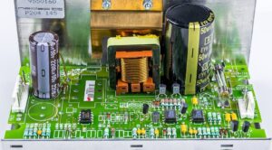
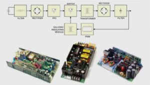
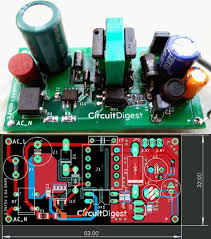
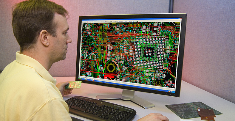
In the switching power supply design PCB board physical design are the last link, if the design method is not appropriate, the PCB may radiate too much electromagnetic interference, resulting in unstable power supply operation, the following for each step of the matters needing attention:
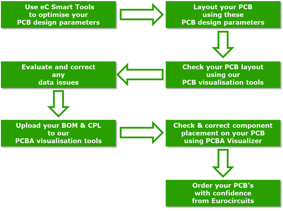
- Design flow from schematic to PCB Create component parameters –> Input schematic netlist –> Design parameter setting –> Manual layout –> Manual wiring –> Verify design –> Review –> CAM output.
- Parameter settings The spacing between adjacent wires must be able to meet electrical safety requirements and should be as wide as possible for ease of operation and production. The minimum spacing should at least be suitable for the voltage withstood. When the wiring density is low, the spacing of signal lines can be increased appropriately, and the signal lines with disparity in high and low levels should be as short and spaced as possible, generally setting the alignment spacing to 8 mil.
The distance from the inner hole edge of the pad to the edge of the printed board should be greater than 1mm, which prevents the pad from being defective during processing. When the alignment connected with the pad is thin, the connection between the pad and the alignment should be designed as a teardrop, which has the advantage that the pad is not easy to skin, but the alignment and the pad is not easy to disconnect. Third, the layout of components practice has proved that even if the circuit schematic design is correct, the printed circuit board is not designed properly, it will also have a negative impact on the reliability of electronic equipment. For example, if the printed board two thin parallel lines close together, it will form a delay in the signal waveform, the formation of reflected noise in the terminal of the transmission line; interference caused by poorly considered power and ground lines will degrade the performance of the product, therefore, in the design of the printed circuit board, attention should be paid to the correct method. Every switching power supply has four current loops:
- Power switch AC loop
- Output rectifier AC loop
- Input source current loop
- Output load current loop
The input loop charges the input capacitor with an approximate DC current, and the filter capacitor primarily acts as a broadband energy storage; similarly, the output filter capacitor is used to store high frequency energy from the output rectifier, while eliminating DC energy from the output load loop. Therefore, the terminals of the input and output filter capacitors are very important. The input and output current circuits should be connected to the power supply only from the terminals of the filter capacitors respectively; if the connection between the input/output circuit and the power switch/rectifier circuit cannot be directly connected to the terminals of the capacitors, the AC energy will be radiated to the environment by the input or output filter capacitors. These two loops are most susceptible to electromagnetic interference, so these AC loops must be laid out before other printed line wiring in the power supply, each The three main components of each loop are filter capacitors, power switches or rectifiers, and inductors or transformers, which should be placed next to each other, adjusting the position of the components so that the current path between them is as short as possible. The best way to create a switching power supply layout is similar to its electrical design, and the best design flow is as follows:
Place the transformer
Designing the power switch current loop
Designing the output rectifier current loop
Control circuit connected to the AC power circuit
Designing input current source circuits and input filters
Designing output load loops and output filters The layout of all components of the circuit according to the functional units of the circuit is based on the following principles:
- First of all, consider the size of the PCB; when the PCB size is too large, the printed lines are long, the impedance increases, the noise immunity decreases, and the cost increases; when it is too small, the heat dissipation is poor and the neighboring lines are susceptible to interference. The optimal shape of a circuit board is rectangular, with an aspect ratio of 3:2 or 4:3. Components located at the edge of the board are generally no less than 2mm from the edge of the board.
- Placement of devices should be considered for future soldering and not too dense.
- Layout is centered around the core components of each functional circuit. Components should be evenly, neatly, and compactly arranged on the PCB to minimize and shorten the leads and connections between each component, with decoupling capacitors as close to the VCC of the device as possible.
- Circuits that operate at high frequencies should consider the distribution parameters between components. In general circuits should be arranged so that components are as parallel as possible. This is not only aesthetically pleasing, but also easy to mount and solder, making it easy to mass produce.
- Place each functional circuit unit according to the flow of the circuit so that the layout facilitates signal flow and keeps the signals in the same direction as much as possible.
- The first principle of layout is to ensure the cloth throughput of wiring, to pay attention to the connection of flying wires when moving devices, and to place devices that have a connection relationship together.
- Minimize loop area as much as possible to suppress radiation interference from switching power supplies.
- Wiring switching power supplies contain high frequency signals. Any printed lines on the PCB can act as an antenna, and the length and width of the printed lines affect their impedance and susceptibility, which affects the frequency response. Even through the DC signal printed lines will be coupled from the adjacent printed lines to the RF signal and cause circuit problems (or even re-radiate the interference signal). Therefore, all the printed lines through the AC current should be designed to be as short and wide as possible, which means that all the components connected to the printed lines and connected to other power lines must be placed very close. The length of the printed line is proportional to the inductance and impedance it exhibits, while the width is inversely proportional to the inductance and impedance of the printed line. The length reflects the wavelength of the printed line response. The longer the length, the lower the frequency at which the printed line can send and receive electromagnetic waves, and the more RF energy it can radiate. According to the size of the printed circuit board current, try to add rent power line width, reduce the loop resistance. At the same time, so that the power line, ground line direction and the direction of the current is the same, which helps to enhance the ability to resist noise. Grounding is the bottom branch of the four current circuits of the switching power supply, as the common reference point of the circuit plays a very important role, it is an important way to control interference. Therefore, the placement of grounding wires should be carefully considered in the layout. Mixing various grounding will cause the power supply to work unstably. The following points should be noted in the design of the ground:
- The correct choice of single point of grounding usually, the common terminal of the filter capacitor should be the only connection point of the other grounding points coupled to the high current AC ground, the grounding points of the same level of circuit should be as close as possible, and the power supply filter capacitor of this level of circuit should also be connected to the grounding point of this level, mainly because the current flowing back to ground in each part of the circuit is variable, because The impedance of the actual flow through the line will lead to changes in the ground potential of each part of the circuit and the introduction of interference. In this switching power supply, its wiring and inductance between the devices have less impact, while the grounding circuit to form a loop current on the interference impact, and thus the use of a point of grounding, that is, the power switch current circuit (in the ground of several devices are connected to the grounding pin, the output rectifier current circuit of several devices ground also received the corresponding filter capacitor grounding pin, so that the power supply work more stable, not easy to self-excitation. When you can’t do a single point, you can connect two diodes or a small resistor at the common ground, in fact, you can connect it at a more concentrated piece of copper foil.
- Try to thicken the ground line If the ground line is very thin, the ground potential changes with the current, resulting in the timing of electronic equipment signal level instability, anti-noise performance becomes bad, so to ensure that each high current ground end using as short and wide as possible printed line, try to widen the power supply, ground line width, preferably wider than the power line, their relationship is: ground line > power line > signal line. If possible, the width of the ground line should be greater than 3mm, but also available in a large area of copper layer for the ground, the printed board is not used in the place are connected to the ground as a ground line.
(1) Global wiring must also follow the following principles The wiring direction: from the soldering surface, the arrangement of the components as far as possible to maintain the same orientation with the schematic diagram, the wiring direction is best consistent with the direction of the circuit diagram alignment, because the production process usually requires the detection of various parameters in the soldering surface, so do so to facilitate the production of inspection, debugging and maintenance (Note: refers to the premise of meeting the circuit performance and the entire machine installation and panel layout requirements).
(2). Design wiring diagram when the alignment as little as possible to turn, the line width on the printing arc do not change abruptly, the corner of the wire should be ≥ 90 degrees, and strive to line simple and clear.
(3). Printed circuit does not allow cross-circuit, for possible cross lines, you can use the “drill”, “around” two ways to solve. That is, let a lead from another resistor, capacitor, transistor foot gap “drill” past, or from the possible cross of a lead end “around” past, in special circumstances how the circuit is very complex, to simplify the design also allows the use of wire spanning, to solve the cross Circuit problems.
3. The input ground and output ground of this switching power supply is a low voltage DC-DC, to feed the output voltage back to the primary of the transformer, both sides of the circuit should have a common reference ground, so after laying copper on both sides of the ground, they should also be connected together to form a common ground.
V. Checking
After the wiring design is completed, it is necessary to carefully check whether the wiring design conforms to the rules set by the designer, and also to confirm whether the rules set meet the requirements of the production process of the printed board. Generally, check whether the distance between the line and line, line and component pad, line and through-hole, component pad and through-hole, through-hole and through-hole is reasonable and whether it meets the production requirements. Whether the width of the power and ground lines are appropriate, and whether there are still places in the PCB where the ground line can be widened. Note: Some errors can be ignored, for example, some of the connector’s Outline part of the board outside the frame, check the spacing will be wrong; in addition, every time you modify the alignment and through-hole, you have to re-copper.
Six, review according to the “PCB checklist”, including design rules, layer definition, line width, spacing, pads, over-hole settings, but also focus on reviewing the rationality of device layout, power, ground network alignment, high-speed clock network alignment and shielding, decoupling capacitor placement and connection.
Seven, the design of the output of the output optical drawing file considerations.
a. The layers to be output are wiring layer (bottom layer), screen printing layer (including top layer screen printing, bottom layer screen printing), solder resist layer (bottom layer solder resist), drilling layer (bottom layer), in addition to generating drilling files (NC Drill)
b. When setting the Layer of the screen printing layer, do not select the Part Type, select the top layer (bottom layer) and the Outline, Text, Linec of the screen printing layer. When setting the Layer of each layer, select the Board Outline, set the Layer of the screen printing layer, do not select the Part Type, select the top layer (bottom layer) and the d. When generating the drill file, use the default settings of PowerPCB and do not change anything.

