1. Introduction
The demand for high-speed digital circuits is increasing every year, as is the need for reliable high-speed PCBs. Digital PCB circuits are compactly packed with microprocessors, power supplies, and many other components that easily operate at frequencies in excess of 1 GHz. these systems are capable of managing billions of operations per second.
The performance of this setup depends on the design phase to optimize any issues that may arise due to high speed operation. Typical problems in high-speed PCB systems include impedance discontinuities, signal reflections, EMI, and noise generation. This article focuses on such issues and techniques to be avoided during the PCB design process.
2. Application of high-speed PCBs
High-speed PCBs are at the heart of computers, smartphones, and other computing devices. These devices are inherently complex. As a result, PCBs are expected to be robust and reliable. The use of high-speed circuits is growing in communications, aerospace, and IoT. Considering the importance of the application, it is important to understand the considerations that must be followed when designing the board layout for high-speed circuits. A typical high-speed system combines technologies such as HDMI, PCI Express, USB or SATA. With these technologies, designers will be able to cope with the limitations of high-speed designs.
3. Design considerations
The following are the preferred techniques for designing high-speed PCBs to enable high-speed operation in low-power environments.
Clock selection and optimization
Minimizing on-board noise in the grid
Minimize crosstalk between signal alignments
Reduces signal reflections
Optimizing systems for EMI form environments and self-coupling
Correct impedance matching and line termination
Floor plan – packing all components
4. Selection of plates
The choice of plate material depends on the dielectric constant and the loss angle tangent of the material. The loss angle tangent is the amount of energy lost from the material as the electromagnetic wave passes through it. The higher the value of the loss angle tangent, the greater the energy loss. The dielectric constant of a material is
εr=ε/ε0
where εr is the dielectric constant, εo is the dielectric constant in free space in (Farad / m), and ε is the material dielectric constant in (Farad / m). The value of εo is approximately 8.85 x 10⁻¹² Farad per meter (F / m). The dielectric constant determines the impedance offered by the material and signals can propagate faster in materials with lower dielectric constants. A typical dielectric material used in PCB designs is FR4. It has a dielectric constant between 4.1 and 4.5 and a loss tangent of 0.019 @ 1MHz.
4.1 Microstrip design
Signal alignments on a single ground plane behave similarly to a microtip layout, while signal alignments between two ground planes act as a ribbon line layout. The characteristic impedance of a microstrip line is given by the following equation
The characteristic impedance of the ribbon line is
To obtain the same impedance value, the dielectric span in a ribbon line layout must be larger than in a microstrip layout, so the ribbon line tends to be thicker than in a microstrip layout.
4.2 Ground plane design
The ground plane in the PCB helps shield, dissipate heat, common reference voltage and reduce stray capacitance. The current in the circuit tends to be reduced in the low impedance path. At very high frequencies, the rapidly rising signal edge couples to the ground layer, which creates a current spike in the ground layer. This current spike can damage the analog performance of the PCB. The presence of a ground plane below can further affect high-speed operational amplifiers as the input stray capacitance increases. To avoid these situations, a proper distance should be maintained between digital devices, analog devices and the ground layer. Less sensitive plated metal can be used as the ground plane.
5. Power and clock design
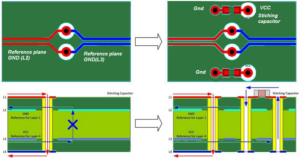
Power supplies are a significant source of on-board low frequency noise in PCB circuits. Power integrity in high-speed systems can be ensured by connecting the power supply layer to the ground layer using shunt capacitors. Parallel capacitors of different values ensure low AC impedance over a wide frequency range. Separate power supply layers should be used for digital and analog devices to minimize noise coupling.
Clock selection is important to ensure that all signals on the PCB layout arrive at the correct time relative to the clock signal. Incorrect clocking can cause problems with rising edge detection or falling edge detection. This will lead to data corruption. The speed of the clock determines the speed of the entire system.
6. Floor plans
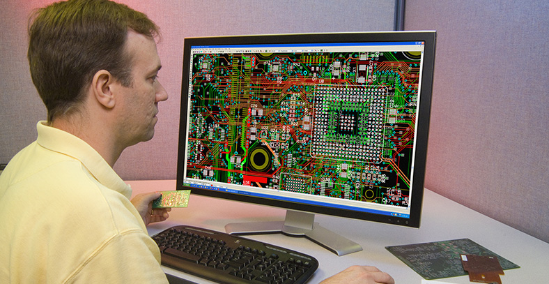
Planning and padding of the floor plan has a significant impact on noise, communication delay, edge rate, and frequency response through parasitic inductance, parasitic resistance, and parasitic capacitance across connecting wires and leads. Chip design, package design and board level design should be completed along with schematic design. The circuit can be laid out in plan view using software simulation prior to physical deployment. Specifying component placement and signal routing from the outset helps designers ensure that the design will work as intended. This reduces cost and rework time, which in turn reduces product cycle time.
7. Signal integrity
PCBs consist of a variety of signals at different frequencies, both analog and digital. These signals are sensitive to noise and coupling. Proper attention must be paid to cabling, shielding, and impedance matching to ensure signal integrity.
7.1 Wiring
The following is a list of certain guidelines to follow during the wiring process
The HF clock alignment should be as straight as possible. Where bends are required, curved bends are preferred over right-angle bends to avoid signal loss due to discontinuities.
Terminate the clock signal, which will help reduce reflections.
Sensitive signal alignments require a high degree of isolation and should therefore be routed on a separate layer.
The long parallel runs of the ribbon lines reduce the distance of signal alignments on the same board. This reduces inductive coupling.
Avoid using multiple vias as they can cause impedance mismatches and increase inductance.
7.2 Impedance matching
Impedance matching between the transmitter and receiver will directly affect the signal integrity. Improper line matching will produce signal reflections and signal loss. The source impedance (ZS) must equal the alignment impedance (Zo) and the load impedance (ZL). Correctly terminating the transmission line ensures matching and signal integrity.
8. EMI optimization
EMI affecting a device can be caused by self-coupling or mutual coupling with other surrounding electronic devices. Certain techniques can be used to optimize EMI in high-speed circuits.
8.1 Matching and wiring
Unmatched or unterminated signal traces can cause reflections. This causes the signal to ring back to the source. Correct matching ensures that signal ringing is eliminated. Correct wiring also reduces self-coupling EMI.
8.2 EMI filters and shielding
Shielding in PCBs is accomplished using a slim ground plane. The skin effect on the conductive surface of the ground plane reduces external EMI, which leads to signal interference in the circuit. EMI filters are used to filter out ambient EMI noise and couple it to ground. A simple decoupling capacitor setup can be used as an EMI filter.
9. Conclusion
In high-speed PCB design, everything must be planned before starting the physical layout process. A good schematic is the foundation for a good layout. Factors such as power supply placement, routing, signal integrity, and impedance matching are important considerations to be addressed during PCB design. Efficient design and implementation will enhance the reliability and robustness of the PCB.

