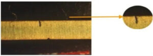
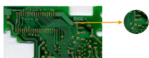
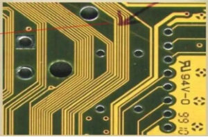
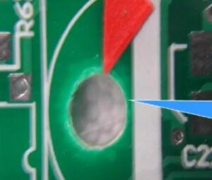
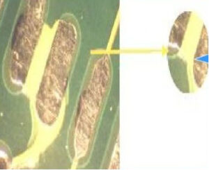
1. Poor substrate and leakage of the bottom plate may cause scratches during transportation, resulting in circuit gaps. Easy to affect the impedance of product wiring. Standardize homework and strengthen control.
2. Poor substrate, localized whitening, improper mechanical impact on the board, or infiltration of fluorinated chemicals into the local board, resulting in etching of the woven points of fiberglass cloth. Electrical connections that may affect appearance and signal. High Tg board is required; Minimize or minimize excessive vibration during machining; Choose the appropriate tin and lead removal solution and operating process.
3. Poor substrate with exposed patterns, caused by low resin content or high fluidity of the bonding film, and excessive adhesive flow during lamination; During lamination, the temperature rises and pressure rises too quickly, and the high pressure is applied too early, resulting in too much glue flow. Impact: Causing a decrease in the insulation performance of the substrate, seriously affecting the quality of the PCB board. Avoidance: The method of “surface material” and “inner material” can be used to increase the resin content of the surface material appropriately and adjust the corresponding technical parameters such as GT and RF%. The product should have sufficient curing temperature and curing time during hot pressing, which can prevent the phenomenon of exposed fabric patterns and improve the chemical resistance and electrical performance of the substrate.
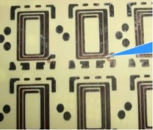
4. Inner layer development is not clean, due to the ink being accidentally exposed during opening, stirring, coating, drying, and drying; Ink is left for too long; Does the drying time meet the requirements? If it is too long, it can easily cause unclear development; Low temperature during development, low concentration of solution, and too fast plate passing speed can all cause impure development. Impact: Causing the lines to be connected together, creating a short circuit and rendering them unusable. It also leads to an open circuit in the circuit, making it unusable. If it cannot be reworked, it will extend the delivery cycle. Avoidance: Ensure that the storage environment of the circuit ink is not exposed to external light; The strong wind during development shall be in accordance with the values specified in the SOP; Adjust the temperature, solution concentration, and plate passing speed according to the parameters of the SOP.
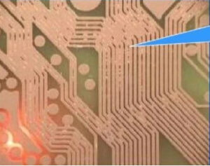
5. The inner erosion plate is not clean, due to the high concentration of chloride ions; The pH value is too low; Insufficient etching pressure; The etching rate is too fast. Impact: This will cause a short circuit, which can also be detected when passing through AOI, and then repaired. Avoidance: reduce the concentration of chloride ions; Increase the pH value; Adjust the etching pressure and etching speed according to the SOP.
6. Inner layer scratches, reason: there is no cross board placement during browning, resulting in scratches; Scratching during the pressing and arranging process. Impact: It affects the appearance, and in severe cases, it may wipe off the circuit, causing an open circuit. Avoidance: Check if the rollers in the water washing and drying sections after browning are too dirty, if there are foreign objects stuck on them, or if the rollers are jumping.
7. Burst hole, cause: The mold punching did not have a guide hole, resulting in the burst hole. Impact: Severe cases can lead to layering, and once layering affects the line, it can cause poor signal quality.
8. Unclean tearing of the film is prone to copper leakage. The reason is that the oxide layer of the copper foil was not treated thoroughly, resulting in poor adhesion after pressing the film, or the electroplating process in the circuit took too long, leading to oxidation of the copper foil in the dry film. Impact: Causing short circuits, repairing thick boards and wires will affect the appearance. Avoidance: If it is caused by grinding the plate, it is necessary to adjust the parameters, as well as the operation method of drying the film, and the tightness of the roller.
9. Penetration plating, reason: poor adhesion between dry film and copper foil leads to penetration plating; The oxide layer of copper foil is not treated cleanly; The process of converting the circuit to electroplating takes too long, resulting in oxidation of the copper foil in the dry film; The water in the electroplating copper cylinder is imbalanced, causing water to attack the dry film and lead to electroplating; During electroplating treatment, the atmospheric pressure is too high or the vibration amplitude of the motor is too large. Impact: It can cause short circuits, open circuits, and is a fatal problem. Avoidance: Choose a good acidic degreaser; Tin plating tank ensures sufficient anode area; Control the amount of tin plating agent in the plating solution to avoid excess; Wet film plated pure tin plates should be stored in a workshop with a relatively good environment, and the storage time should not exceed 72 hours.

