High-speed PCB design is any design where signal integrity starts to be affected by physical characteristics of the PCB, such as layout, packaging, interconnects, and layer stacking. And, when you start designing boards and run into trouble with things like delays, crosstalk, reflections, or emissions, you’re entering the realm of high-speed PCB design.
High-speed designs are so unique because of the focus on these issues. You may be used to designing a simple PCB that focuses primarily on component placement and routing. However, when working with high-speed designs, it is more important to consider factors such as their distance from the signal, the width of the signal, the location of the placed traces, and the type of traces they are connected. In addition, by taking these factors into account, it will reach a higher level in your PCB design process.
High-speed PCB design tips
1. Know the design software that offers advanced options
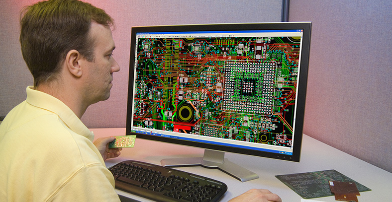
It takes a lot of sophistication to design at high speed in CAD software. Also, there may not be many programs for hobbyists, and there are usually no advanced options based on the Web Suite. Therefore, you need to have a better understanding of powerful CAD tools.
2. High-speed routing
When it comes to high-speed routing, designers need to understand the rules of basic routing, including not cutting off ground layers and keeping the routing short. Therefore, prevent crosstalk over some distance on digital lines and shield all interference generators from damaging signal integrity.
3. Alignment with impedance control
For some signals of about 40-120 ohms, it requires impedance matching. The hints for characteristic impedance matching are the antenna and many differential pairs.
It is important for designers to understand how to calculate the alignment width and the necessary impedance values for the stack. If the impedance values are incorrect, this can have a serious impact on the signal, which can lead to data corruption.
4. Length-matching traces
There are many lines in the high-speed memory bus and interface bus. These lines can operate at very high frequencies, so it is critical that the signal must travel from the transmitter to the receiver simultaneously. In addition, it requires a feature called length matching. Therefore, the most common standards define the tolerance values that need to be matched to the length.
5. Minimizing loop area
High-speed PCB designers need to know a few tricks. High-frequency signals can cause EMI, EMC, and other problems. Therefore, they need to follow basic rules, such as having continuous ground layers and reducing loop area by optimizing the current return path of the alignments, and putting in many stitched vias.
High-speed PCB design considerations
PCB layout is very important
There is no doubt that efficient PCB fabrication in high-speed circuits is important to the end result. However, this process does not consider PCB layout in the first place. As a result, it will have a significant impact on the design to achieve the necessary functionality and successful PCB manufacturing, such as performing high-level planning and adhering to important factors. In addition, you need to address issues such as design for manufacturing (DFM) practices and additional considerations for high-speed PCB requirements prior to PCB layout.
Bad layouts can lead to performance issues when starting testing or for PCB manufacturing. Even worse, it takes more cost and time to redesign or rework because of the need to evaluate PCB failures or performance issues and reassemble prototype layouts.
PCB design considerations
In fact, high-speed PCB design places many constraints on designers as you need to meet a variety of signal speeds and other design requirements. Therefore, there are a number of factors to consider to achieve a high-speed board design as shown below:
Principal diagram considerations: It is well known that a good schematic can be a good foundation for a PCB design. Therefore, depending on whether you are a PCB designer or an electrical engineer, the schematic can be treated differently. Usually, it treats the schematic as a way of communication that can be connected to the board. But schematics can have a big impact on organizing and presenting your high-speed designs. Therefore, it is important to have as much information available on the design schematic as possible, such as alignment lengths, necessary component placement, PCB manufacturer information, etc.
Trace length adjustment: When using a high-speed interface, you need to adjust the trace length to synchronize the signal transmission with the data line. However, the interface may fail at the maximum frequency or may not work at all because it is not synchronized. Moreover, the higher the interface frequency, the higher the length matching requirement. Therefore, in the case of a parallel interface, you only need to adjust the length of all alignments. It is important to be sure to adjust the lengths of these alignments to get the desired length in a set of signals.
PCB materials and requirements for high-speed stacking: This will affect your high-speed design, such as the structure of the layer stack and the material of the PCB.
High-speed placement strategy: Since changing pad sizes and component gaps can minimize high-speed connection lengths, it allows for high-speed design using a variety of methods to optimize component placement and improve the footprint of components to achieve high speed.
Differential pair and alignment length routing: It is important to route differential pairs in high-speed designs so that pairs of signals can exist simultaneously.
Crosstalk, impedance control, and parallelism considerations: There are many factors that can adversely affect your design in a high-speed design. There are also a number of techniques to consider, such as how to minimize the impact on your design.
Understanding ribbon and microstrip lines: Typically, for high-speed designs, it requires multiple methods of routing alignments. If you want to implement high-speed routing, it is best to have a better understanding of ribbon wire and microstrip routing technologies.
Wiring topologies and best wiring practices: Often, a specific shape or topology needs to be used if the circuit path required for high-speed wiring is to be achieved. And it’s great to explore various ways to keep track of alignment lengths, escape characters, return paths, etc.
Simulators: For high-speed designs, simulation can be very beneficial before, during, and after the layout begins. Therefore, you should have a better understanding of PCB design software to learn tips and tricks to use for simulating your design.
How do you know if you need a high-speed PCB design?
1. Is there a high speed interface on the board?
A quick way to find out if you need to follow high-speed design guidelines is to check if you have a high-speed interface such as DDR, PCI-e, or even a video interface such as DVI, HDMI, etc.
All of these interfaces need to follow some high-speed design rules. In addition, please provide the exact specification of each data in the documentation.
2. Ratio of trace length to signal wavelength
Usually, if the wavelength of your message is the same as the length of the trace, then your PCB will definitely require a high-speed design. This is because certain standards, such as DDR, require the length of the alignment to match the minimum tolerance.
A good rough number is if your alignment length and wavelength can be controlled to within an order of magnitude of each other. Then, it is best to check
