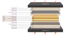
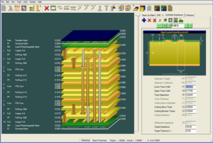
In general, the PCB stack design to comply with the two main rules:
- each alignment layer must have a neighboring reference layer (power or ground layer);
- adjacent to the main power supply layer and ground layer to maintain a minimum distance to provide a larger coupling capacitance;
Listed below are examples of stacked layers from two-layer to eight-layer boards to explain.
A, single-sided PCB board and double-sided PCB board stacking
For two-layer board, due to the small number of board layers, there is no longer a problem of stacking. Control EMI radiation mainly from the wiring and layout to consider.
Single- and two-layer boards are increasingly prominent EMC problems. The main reason for this phenomenon is due to is the signal circuit area is too large, not only produces a strong electromagnetic radiation, but also makes the circuit sensitive to external interference. To improve the electromagnetic compatibility of the line, the easiest way is to reduce the circuit area of the critical signal.
Key signal: From the perspective of electromagnetic compatibility, the key signal mainly refers to the signal that generates strong radiation and the signal that is sensitive to the outside world. Signals that generate stronger radiation are generally periodic signals, such as clocks or low signals of addresses. Signals that are sensitive to interference are those analog signals with lower levels.
Single and double layer boards are usually used in low frequency analog designs below 10KHz:
1) power supply alignment on the same layer in radial form and minimizing the sum of line lengths.
2) go power and ground lines close to each other; lay a ground line on the edge of the key signal line, this ground line should be as close as possible to the signal line. This creates a smaller loop area, reducing the sensitivity of the differential mode radiation to external interference. When the signal line next to the addition of a ground line, the formation of a minimum area of the loop, the signal current will certainly take this loop, rather than other ground path.
If it is a double-layer circuit board, the other side of the circuit board, close to the signal line below, along the signal line cloth a ground line, a line as wide as possible. This forms a circuit area equal to the thickness of the circuit board multiplied by the length of the signal line.
Second, the four-layer board lamination
- SIG – GND (PWR) – PWR (GND) – SIG.
Segment
- GND-SIG(PWR)-SIG(PWR)-GND.
For the above two stacked layer designs, the potential problem is for a conventional 1.6mm (62mil) board thickness. Layer spacing will become very large, not only is not conducive to control impedance, inter-layer coupling and shielding; in particular, the spacing between the power ground layer is large, reducing the board capacitance, which is not conducive to filtering noise.
For the first scheme, usually applied to the case of more chips on the board. This scheme can get better SI performance, for EMI performance is not very good, mainly through the alignment and other details to control. The main attention: the ground layer is placed in the most dense signal layer connected to the layer, which is conducive to the absorption and suppression of radiation; increase the board area, reflecting the 20H rule.
For the second program, usually applied to the board chip density is low enough and the chip has sufficient area around (to place the required power cladding layer) occasions. The outer layer of this scheme PCB are ground layer, the middle two layers are signal / power layer. Signal layer on the power supply with a wide line alignment, which can make the path of the power supply current impedance is low, and the signal microstrip path impedance is also low, but also through the outer layer of ground shielding the inner layer of signal radiation. From the point of view of EMI control, this is the best available 4-layer PCB structure.
Main attention: the middle two layers of signal, power supply mixed layer spacing to be pulled apart, the alignment direction vertical, to avoid crosstalk; appropriate control of the board area, reflecting the 20H rule; if you want to control the alignment impedance, the above scheme to be very careful to lay the alignment in the power supply and grounding copper island under the edge. In addition, the copper laying on the power supply or ground should be interconnected together as much as possible to ensure DC and low frequency connectivity.
Three, six-layer stacking of panels
For designs with higher chip densities and higher clock frequencies a six-layer board design should be considered with the recommended stacking method:
1. SIG-GND-SIG-PWR-GND-SIG;
For this scheme, this stacked layer scheme gives better signal integrity, the signal layer is adjacent to the ground layer, the power layer and ground layer are paired, the impedance of each alignment layer can be better controlled, and both ground layers are good at absorbing magnetic lines. The power and ground layers are intact and can provide a good return path for each signal layer.
2. GND-SIG-GND-PWR-SIG -GND;
For this scenario, which is only suitable if the device density is not very high, this stack has all the advantages of the above stack, and the top and bottom ground planes are more complete so it can be used as a better shield. It should be noted that the power supply layer to be close to the non-main component side of the layer, because the bottom layer of the plane will be more complete. Therefore, the EMI performance is better than the first option.
Summary: For a six-layer board solution, the spacing between the power and ground layers should be minimized to obtain good power and ground coupling. However, with a 62 mil board thickness, the spacing between the layers is reduced, but it is still not easy to control the spacing between the main power and ground layers to be small. Comparing the first solution with the second one, the cost of the second solution is much higher. Therefore, we usually choose the first option when stacking layers. The design follows the 20H rule and the mirror layer rule.
Four, eight-layer stacking of panels
1. This is not a good stacking method due to poor electromagnetic absorption and large power impedance. It has the following structure:
1.Signal 1 Component face, microstrip layer2.Signal 2 Internal microstrip layer, better alignment layer (X-direction) 3.Ground4.Signal 3 Ribbon alignment layer, better alignment layer (Y-direction) 5.Signal 4 Ribbon alignment layer 6.Power7. Wire alignment layer 8.Signal 6 Microstrip wire alignment layer
2. A variant of the third stacking method, with better EMI performance due to the addition of a reference layer, and the characteristic impedance of each signal layer can be well controlled
1. Signal 1 component surface, micro stripe layer, good alignment layer
2. Ground layer, good electromagnetic wave absorption
3. Signal 2 ribbon cable alignment layer, good alignment layer
4. Power Power layer, which forms an excellent electromagnetic absorption with the ground layer below 5. Ground layer
6. Signal 3 Ribbon alignment layer, good alignment layer
7. Power ground with large power impedance
8. Signal 4 micro strips with wire layer, good alignment layer
3. Best stacking method, very good geomagnetic absorption due to the use of multiple ground reference planes.
1. Signal 1 component face, micro walk away layer, good alignment layer
2. Ground layer, good electromagnetic wave absorption
3. Signal 2 ribbon alignment layer, good alignment layer
4. Power Power layer, which forms excellent electromagnetic absorption with the strata below 5. Ground layer
6. Signal 3 ribbon alignment layer, good alignment layer
7. Ground stratum, better electromagnetic wave absorption
8. Signal 4 micro walk away layer, good alignment layer
The choice of how many layers to use and what kind of stack to use for a design depends on the number of signal networks on the board, device density, PIN density, signal frequency, board size, and many other factors. We need to consider all these factors together. For the number of signal networks, the greater the device density, the greater the PIN density, the higher the frequency of the signal design should try to use multilayer board design. To get good EMI performance it is best to ensure that each signal layer has its own reference layer.

