Top 10 PCB routing tips for beginners
There is an old saying that PCB design is 90 percent layout and 10 percent routing. This is still true today, and the placement of components will ultimately determine how much time the cabling will take, but that doesn’t mean that wiring the PCB is any less important. It’s just a matter of how much time you spend on each activity.
If this is your first PCB layout, it can be a little intimidating to see what chaos looks like. Use these top 10 PCB routing tips along with our top 10 component placement tips to make your first PCB layout a success.
Tip #1 – Don’t rely on your autowire
Almost all PCB design software has a tool called an autorouter, and as a beginner, you might think it’s an easy way to solve your wiring problems and light up. But wait! The best possible autorouter will never replace doing your own wiring, and should only be used for several reasons, including:
Accuracy. After placing all components, you can use the auto-routers to see the finish level obtained. If it is below 85%, then you need to make some adjustments to the part positions.
Bottlenecks. You can also use the autowire to discover bottlenecks and other critical connection points that may not have been seen during component placement.
Inspiration. Finally, you can use the autowire as a source of inspiration for how to wire some of the traces you were unable to complete. A quick glance at the autowire may show you new paths that you never considered before.
In addition to these three reasons, we recommend not relying on autowiring for all the wiring for the layout on the board. Why? It’s not always the most accurate, and if you’re a symmetry enthusiast, your autorouter will likely be disappointing. And most importantly, you are the master of your design and can complete the wiring process yourself to produce better results. It’s a carefully designed process that requires a certain amount of love and attention to get the results you want.
Tip #2 – Know the manufacturer’s specs
Before you start laying copper alignments, take the time to call or email the manufacturer to see if they have any specific requirements for minimum alignment widths, alignment spacing, and the number of layers they can handle. Board (at the right price)
Why? By knowing this information up front, you can set the alignment width and spacing values in your design rules without having to rewire the entire board layout. By using the alignment widths and spacings that manufacturers can produce, it makes everyone’s life easier when building boards.
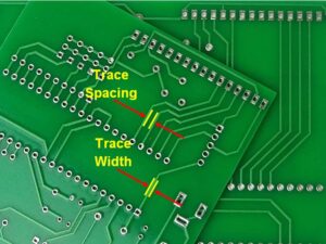
Tip #3 – Find the trace width
As you traverse all the copper traces with increasing current, it will generate some serious heat, which is always a concern with electronic devices. Controlling the width of the traces is one of many ways to reduce the amount of heat that builds up on the board; the wider the traces, the less resistance there is to flow through the circuit.
To determine the thickness of the alignment, you can use a handy alignment width calculator like Advanced Circuits, which will allow you to plug in the estimated current and thickness and get the alignment width values for the internal and external layers. A word of advice – if you have the opportunity to use an alignment width wider than the calculator shows, go for it! As long as the manufacturer’s requirements are met, then the larger the alignment, the less likely it is that a broken board will be recovered.
Tip 4 – Leave enough space between traces
Be sure to leave enough space between all the traces and pads in the PCB layout. Why? If you bundle everything too tightly, you run the risk of short circuits when building the board and unintentionally connecting the alignments.
Remember that the PCB manufacturing process is not 100% accurate, so you always need to leave some margin between component pads and alignments to stay safe. As a minimum requirement, we recommend always leaving 0.007″ to 0.010″ of clearance between all adjacent pads and alignments on the board.
Tip #5 – Use the capture grid to make your work easier
In Autodesk EAGLE, you have full control over the snap grid settings, which is handy during component placement and routing. There’s no reason not to turn on visible grid snapping, which you’ll appreciate later when you start working with more dense board layouts that require precise placement of traces and parts.
As a guideline, we recommend setting the capture grid spacing to 0.050″ during the wiring process. Alternative spacing can also be set to 0.025″ when closely spaced connections between components need to be designed. Of course, always set the visible grid to “on”!
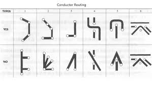
Tip #6 – Avoid using 90 degree alignment angles
If you talk to engineers and manufacturers, you will hear over and over again, don’t use 90 degree alignment angles. Why? When you have a bundle of sharp, right-angle-turned alignments on your board, the outer corners of that 90-degree angle may be etched narrower than the standard alignment width. And in the worst case scenario, you could get a bunch of 90 degree traces that are not fully etched, which could lead to a short circuit.
As a solution to this problem, try using 45 degree angle traces. This will produce some nice PCB layouts while still being able to easily etch off all the copper on the board, thus making the manufacturer’s job easier.
Tip #7 – Leave space between the alignment and mounting holes
During component placement, you may have placed all the mounting holes first, but did you throw them down, leaving enough space between the other components and all the alignments that connect them together? If you don’t, you may risk creating a shock hazard on the board, and relying on the solder-resistant layer as the only insulator does not guarantee safety. Therefore, when using mounting holes, always remember to leave some space outside of the physical dimensions of the mounting holes to prevent them from being affected by other components and nearby traces.
Tip #8 – Always create a ground wire
There must be a common ground on the PCB because it provides the same reference point for measured voltage for all alignments. This will come in handy if you are going to use an analog circuit as your first design. If you use alignments for grounding instead of grounding layers, you will find many different ground connections on the board, all of which have their own resistance values and voltage drops, which can be a nightmare.
To avoid all this nonsense, we always recommend that you create a dedicated grounding layer on your PCB layout. This could be a large copper area on a single layer board, or even an entire layer dedicated as a ground plane on a multilayer board. Once the grounding layer is added, simply connect all the components that need to be grounded through the vias.
Tip #9 – Expand power and ground alignment
Not all alignments on a PCB layout are the same, and you need to make sure to increase the width of the alignments that will be used as power and ground paths. Why? Both power and ground paths will flow more current, and if you don’t make them wider than usual, they will flow through these narrow spaces giving off a lot of heat, which can eventually burn up the wires and destroy your equipment and boards.
By making the power alignment and ground alignment as thick as possible, you can also quickly identify the design if you need to view and adjust it in the future.
Tip 10 – Use through-hole cooling
Our final tip has to do with vias, which seem to be the masterpiece of all trades when it comes to PCB layout. Not only are vias ideal for providing electrical connections between layers, but they are also ideal for when heat needs to be transferred from one side of the board to the other.
This comes in handy if you need to conduct heat away from a super power component, such as an integrated circuit (IC). By placing multiple vias under the core of the IC, you can reduce the operating temperature of the component, which will make your design more reliable in the long run.
Move on!
Even the best component placement can become meaningless if you don’t take the time to think about how to plan all the alignments. Did you remember to give all the ICs enough room to connect all the pins? Is there enough room for all those mounting holes? Considering all of these questions and more will help you successfully complete your first PCB design flow. Just like the component placement process, you may find


