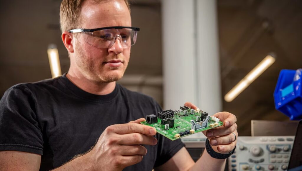
1. Principles of Printed Circuit Boards. Printed Circuit Board (PCB), also known as circuit boards, PCB boards, aluminum boards, high frequency boards, ultra-thin boards, thin boards, and printed (copper etching technology) boards are important electronic components that support electronic components and are providers of dedicated lines for connecting electronic components. Traditional circuit boards, the circuit diagrams and drawings of circuits are made by printing resist, and are therefore called printed circuit boards and printed circuit boards. As electronic products will continue to be fine, most circuit boards are currently affixed to the attached resist (laminated or coated) and exposed for development before the circuit board can be etched. 1. Structure circuit boards are mainly composed of pads, holes, mounting holes, wires, components, connectors, fillers, electrical boundaries. Common board layer structures include single board (single layer PCB), dual board (double layer).

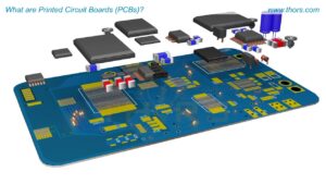
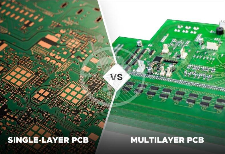
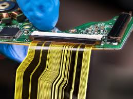
2. PCBs and multilayer boards. The main functions of each component are as follows: Pads: metal holes for soldering component pins. Through holes: metal through holes and non-metal through holes where metal holes are used to connect pins between components on each layer. Mounting holes: Used to fix the board. Conductor: Copper film network used to connect component pins. Connectors: Used to connect components between circuit boards. Filling: The copper wire applied to the ground network can effectively reduce impedance. Electrical Boundary: Used to size the board so that all components on the board do not exceed the boundary.

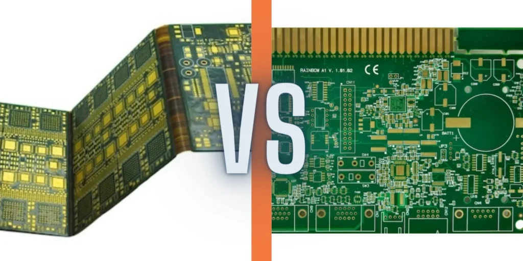
3. PCBs work by separating the substrate insulation material from the conductive copper foil surface layer, allowing various components such as the stream to perform, amplify, attenuate, modulate, demodulate, and encode functions when the fronts are pre-designed with wires. On the basis of the PCB, the parts are on one side and the wires are concentrated on the other side. Because the conductors appear only on one side, the PCB is called a single board. Multi-layer boards and multi-layer wires must have proper circuit connections between them, and the bridge between the circuits is called a pilot hole (through-hole), between the two layers. The process of circuit board design can be divided into the following four steps:
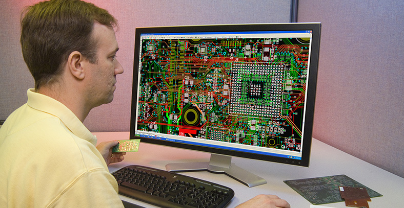
(1) Circuit schematic design — Circuit schematic design is mainly to draw schematics using DXP Protel Schematic Editor.
(2) Generated Web Forms – Web reports are links between circuit schematics and components displayed in each report, which bridges and links circuit schematic designs and board designs through the web. The reports make it easy to find connections between components quickly, thus providing easy access to the back of the PCB design.
(3) printed circuit board design, printed circuit board design is often referred to as PCB design, it is the conversion of the circuit schematic into its final form, this part of the design is circuit schematic design is very difficult, we can Protel DXP powerful design features can be completed in this part of the design.
(4) Generate printed circuit board tables. Once the printed circuit board design is complete, various reports need to be generated, such as generating pin declarations, board information reports, network status reports, and finally printing out the printed circuit board.
