1. Bare copper plate
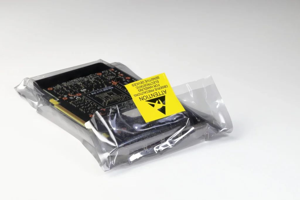
The advantages and disadvantages are obvious:
Pros: low cost, flat surface, good weldability (when not oxidized).
Downside: susceptible to acid and humidity, can’t be stored for long, need to be used up within 2 hours after unpacking because copper is easily oxidized when exposed to air; can’t be used for double-sided boards because the second side is already oxidized after the first reflow. If there are test points, solder paste must be added to prevent oxidation, otherwise the subsequent will not be able to make good contact with the probe.
Pure copper is susceptible to oxidation if exposed to air, and the outer layer must have the aforementioned protective coating. So it requires surface treatment in the circuit board processing.
2. OSP process board
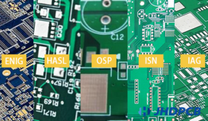
OSP differs from other surface treatment processes in that it acts as a barrier between copper and air. Simply put, OSP is an organic film that chemically grows on a clean, bare copper surface. Because it’s organic, not metal, it’s cheaper than the spray tin process.
The only purpose of this film of organics is to keep the inner copper foil from oxidizing prior to soldering. Once heated during soldering, this film evaporates away. Solder is then able to solder the copper wire and components together. But this layer of organic film is very resistant to corrosion, an OSP circuit board, exposed to the air for ten or so days, you can not solder components. Computer motherboards have a lot of OSP process. Because the board area is so large, OSP is more economical.
Benefits: All the advantages of soldering bare copper, and expired boards can be resurfaced once again.
Disadvantages: 1. OSP is transparent and colorless, so it is difficult to check and identify whether it has been treated with OSP. 2. OSP itself is insulating and non-conductive, which can affect electrical testing. OSP can not be used as an electrical contact surface, such as the keypad surface of the keypad. 3.OSP is easily affected by acid and temperature. When used in secondary reflow, it needs to be completed within a certain period of time, usually the second reflow will be less effective. If the storage time exceeds three months, the surface must be re-treated. The product must be used within 24 hours after opening the package.
3. Hot Air Leveling (HASL)
Hot air leveling, also known as hot air solder leveling, is a process of coating the surface of a PCB with molten tin-lead solder and leveling (blowing) it with heated compressed air to form a coating layer that resists copper oxidation and provides good solderability. Hot air leveling forms a copper-tin metal compound at the bond between the solder and copper, which is approximately 1 to 2 mil thick.
Wave soldering is the best soldering method where perforated devices dominate, and HASL is sufficient for wave soldering processes, although of course nickel/gold plating is mostly used for high junction strength requirements.
Advantages: low cost
Downside: 1. HASL technology treated pads are not flat enough and coplanarity does not meet the process requirements for fine pitch pads. 2. Not environmentally friendly, lead is harmful to the environment.
4. Gold Plated Boards
Gold plating uses real gold, and even with a very thin layer, it already accounts for nearly 10% of the cost of the board. The use of gold as a plating layer is for ease of soldering and to protect against corrosion. Even the gold fingers of memory sticks that have been used for years are still shiny as ever. If copper, aluminum, or iron had been used for the same amount of time, they would have rusted to a pile of scrap by now.
Gold plating is used extensively on circuit boards for component pads, gold fingers, connector tabs, and other locations. Most of the motherboards of our most widely used cell phone boards are gold plated and sunken, while computer motherboards, audio and small digital boards are generally not gold plated.
Benefits: High electrical conductivity, good oxidation resistance, long life. The plating is dense and relatively wear-resistant, typically used for bonding, soldering and plugging.
Cons: Higher cost and poorer weld strength.
5. Enigmatic gold/submerged gold (ENIG)
Electroless Nickel Immersion Gold (ENIG), also known as Electroless Nickel Gold, Immersion Nickel Gold, or simply Electroless Gold and Immersion Gold, is a thick, electrically good nickel-gold alloy that is chemically wrapped around the copper surface and protects the PCB for a long time. the inner layer of nickel is typically deposited at a thickness of 120~240μin (about 3~6μm), and the outer layer of gold is typically deposited at a thickness of 2~4μinch ( 0.05~0.1μm). Not like OSP only as a rust barrier layer, it can be useful and achieve good electrical properties during the long-term use of PCB. It also has the environmental tolerance that other surface treatment processes do not have.
Benefits: 1. ENIG-treated PCB surface is very flat and coplanar, suitable for key contact surfaces. 2. ENIG has excellent solderability, the gold will quickly blend inside the melted solder, and the solder forms a Ni/Sn metal compound with Ni.
Disadvantages: The process is complex and requires tight control of process parameters to achieve great results. The most troublesome part is that the EING treated PCB surface is prone to black disc benefits during ENIG or soldering. The immediate manifestation of black disk is excessive Ni oxidation and too much gold, which can make solder joints brittle and affect reliability.
6. Electroless nickel-palladium-impregnated gold (ENEPIG)
Compared to electroless nickel-gold, ENEPIG has an additional layer of palladium between nickel and gold. During the deposition reaction of the replacement gold, the electroless palladium layer protects the nickel layer from excessive corrosion by the replacement gold, and the palladium prepares it for immersion in gold while preventing corrosion due to the replacement reaction. The deposition thickness of nickel is generally 120~240μin (about 3~6μm), the thickness of palladium is 4~20μin (about 0.1~0.5μm). The deposited thickness of gold is typically 1 to 4 μin (0.02 to 0.1 μm).
Benefits: It has a wide range of applications, while the chemical Ni-Pd-Au finish can replace Ni-Pd-Au by effectively preventing the connection reliability problems caused by Black Pad defects compared to the Ni-Pd-Au finish.
Cons: Although ENEPIG has many advantages, palladium is expensive and is a shortage resource. It also has the same stringent process control requirements as nickelized gold.
7Tin-sprayed circuit boards
A silver-colored board is called a spray-tin board. Spraying a layer of tin on the outer layer of copper’s wiring can also help with soldering. But it does not provide the long term contact reliability that gold does. It has little effect on components that are already soldered, but is not reliable enough for pads that are exposed to air for long periods of time, such as ground pads, poppet sockets, etc. Long-term use is prone to oxidation and rust, resulting in poor contact. Basically, the circuit board used as a small digital product is invariably a spray-tin board, the reason being that it is cheap.
Benefits: Lower price and good welding performance.
Disadvantages: Not suitable for soldering fine-gap pins and components that are too small because of the poor surface flatness of the sprayed tin plate. Solder beads are easily generated in the PCB process, which can cause short circuits on fine pitch components. When used in a double-sided SMT process, because the second side has been reflowed at a high temperature, it is very easy to melt the spray tin again and produce tin beads or similar water beads affected by gravity into drops of spherical tin dots, resulting in a more uneven surface and thus affecting the soldering problem.
8Silver dip
The silver immersion process is intermediate between OSP and chemical nickel/gold immersion, and is a simpler and faster process. Silver immersion is a displacement reaction, which is almost a submicron coating of pure silver (5 to 15 μin, about 0.1 to 0.4 μm). Sometimes the silver immersion process also contains some organic matter, mainly to prevent silver corrosion and eliminate silver migration problems, it is generally difficult to measure this thin layer of organic matter, analysis shows that the weight of the organic body is less than 1%. Even when exposed to heat, humidity and pollution, it still provides good electrical properties and maintains good solderability, but loses its luster. Because there is no nickel underneath the silver layer, immersion silver does not have all the good physical strength of chemical nickel/immersion gold plating.
Benefits: The silver dip solder surface is well solderable and coplanar, while not as conductive as OSP, but not as strong as gold when used as a contact surface (e.g., a key surface).
Disadvantages: One important issue with silver immersion is the electron migration of silver, which can be reduced by adding organic components to the silver in response to voltage when exposed to moisture.
9Tin dipping
Since all current solders are tin-based, the tin layer can be matched to any type of solder. However, previous PCBs were prone to tin whiskers after the immersion tin process, and tin whiskers and tin migration during soldering can cause reliability issues, thus limiting the adoption of the immersion tin process. Later, organic additives were added to the immersion tin solution to give a granular structure to the tin layer, overcoming the previous problems, and also providing good thermal stability and solderability.
The biggest weakness of immersion tin is its short life, especially when stored in high temperature and high humidity environments, where the Cu/Sn intermetallic compound grows until it loses solderability. A tin deposit thickness of no less than 40 μin (1.0 μm) is reasonable to provide a pure tin surface for solderability requirements.
Disadvantages: The biggest weakness of immersion tin is its short lifespan, especially when stored in high temperature and high humidity environments, where the Cu/Sn intermetallic compound grows until it loses solderability. There is also no diffusion problem between electroless nickel/impregnated gold metals; only that immersion tin plates cannot be stored for too long.

