We move on to talk about the PCB manufacturing process.
PCB Production Step 3: Printing the inner layer: where will the copper flow?
The development in the previous step was designed to draw a copper line graphic. Now it’s time to print the graphics on the film onto the copper foil.
This step in PCB manufacturing prepares the actual PCB. the basic form of a PCB is a laminate with a core of epoxy resin and glass fiber, also known as a substrate. The laminate is the ideal body to receive the copper that makes up the PCB. The substrate material provides a strong and dustproof starting point for the PCB. The copper is pre-bonded on both sides. The process involves chipping away at the pattern on the copper.
Cleanliness is critical in PCB construction. Clean the copper side laminate and then feed it into a clean environment. At this stage, it is critical that no dust particles are deposited on the laminate. Erroneous stains can cause circuits to short out or remain disconnected.
Next, the clean panel receives a photosensitive film layer called a photoresist. The photoresist includes a layer of photoreactive chemicals that hardens after exposure to UV light. This ensures an exact match from photographic film to photoresist. The film is mounted in the proper position for securing the pins to the laminate.
The film and cardboard are lined up and receive a beam of UV light. The light passes through the transparent part of the film and hardens the photoresist on the copper underneath. The plotter’s black ink prevents the light from reaching the undesired hardened areas, so it is removed.
After the board is prepared, it is washed with an alkaline solution to remove any unhardened photoresist. A final pressure wash will remove anything else left on the surface. The board is then dried.
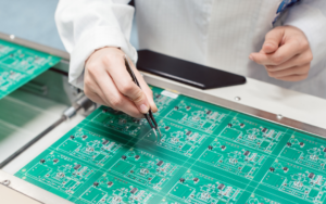
The product emerges with a resist that properly covers the copper areas to be retained in the final form. The technician checks the board to ensure that no errors have occurred at this stage. All resist present at this point indicates the copper that will be exposed in the finished PCB.
This step is only applicable to boards with more than two layers. Simple two-layer boards can be skipped for drilling. Multi-layer boards require more steps.
Step 4: Fading copper
After removing the photoresist and covering the copper we want to keep with hardened photoresist, the board moves on to the next stage: removing the unwanted copper. Just as the alkaline solution removes the resist, the more powerful chemistry consumes the excess copper. The copper solvent solution bath removes all bare copper. At the same time, the desired copper remains fully protected beneath the hardened layer of photoresist.
Not all copper boards are created equal. Some heavier boards require a lot of copper solvent and variable exposure times. As a side note, heavier copper boards require special attention to track spacing. Most standard PCBs rely on similar specifications.
Now that the solvent has removed the excess copper, the hardened resist that protects the preferred copper needs to be washed off. Another solvent can accomplish this task. The board now flashes with only the copper substrate required for the PCB.
Step 5: Layer alignment and optical check
As all the layers are cleaned and prepared, the layers need to align the punch holes to make sure they are all lined up. Aligning the holes aligns the inner layers with the outer layers. The technician puts the layers into a machine called an optical punch, which allows for precise correspondence so that the holes can be punched accurately.
Once the layers are put together, it is impossible to correct any errors that occur in the inner layers. Another machine performs an automatic optical inspection of the panel to confirm that it is completely free of defects. The manufacturer receives the original design of the Gerber as a model. The machine scans the layers using a laser sensor and then electronically compares the digital image with the original Gerber file.
If the machine finds an inconsistency, the comparison is displayed on the monitor for the technician to evaluate. Once the layer passes inspection, it will move to the final stage of PCB production.
Guangzhou Jujin Technology will continue to talk about the process of PCB production in the following, looking forward to your attention!

