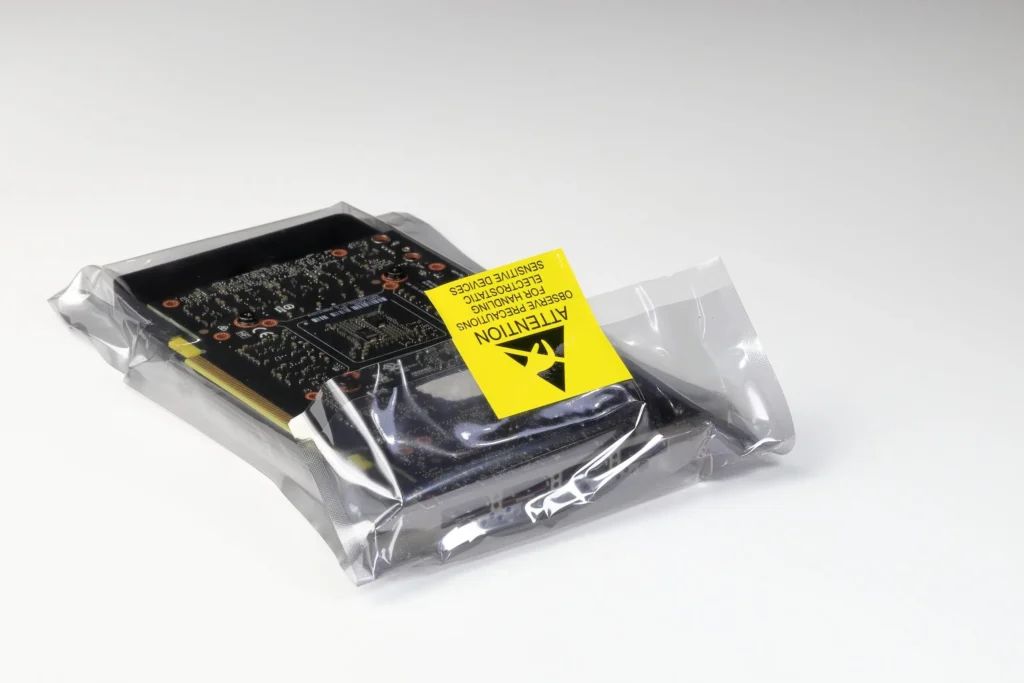
Depending on the manufacturer of the printed circuit board, a variety of methods can be used to design the PCB. The board design can be mass produced using multiple machines in the PCB manufacturing industry, including drilling, punching, plating and final manufacturing processes performed by highly automated machines. High quality PCBs (with higher production yields) can be produced using CNC machines, automated plating machines, stripping etching machines for laser punching, and optical inspection equipment, flying probe testers for electrical testing of printed circuit board processes.
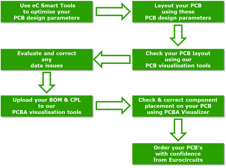
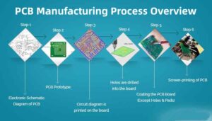
To help the reader understand the concept at a basic level of PCB design, the following step-by-step process for designing PCBs at each level will help and guide you.
Step 1: Designing a PCB circuit using software
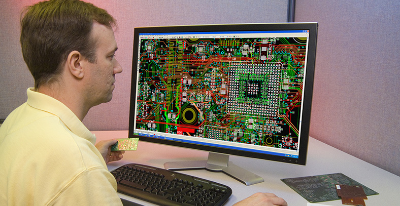
Draw schematics using PCB layout software such as CAD software, Eagle and Multisim software. This type of PCB design software contains libraries of components that can be used to build circuits. It is also possible to change the location of the circuit design and then modify it according to your convenience and requirements. Here, we have chosen Eagle software to design the circuit, and the process is as follows:
Open the Eagle board design software.
Window with menu bar appears.
Click on the File menu.
Select “New Design” from the drop-down menu.
Click on the Library menu.
Select “Select device/symbol” from the drop-down menu.
Double-click to select an associated annotation so that the component appears in the window.
Add all the components and draw a properly connected circuit as shown.
Enter the level of each component as required.
Go to the command toolbar, then click Text Editor Variables, click Variables, and close the window.
Next, a black screen appears, as shown below, which is the layout or film diagram of the circuit, and saves it in image format.
Step 2: Graphics transfer
The film is generated from the final circuit diagram from the PCB layout software, which is sent to the manufacturing cell where the negative image or mask is printed on the plastic board.
Step 3: Select raw materials
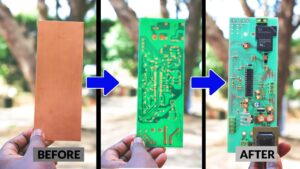
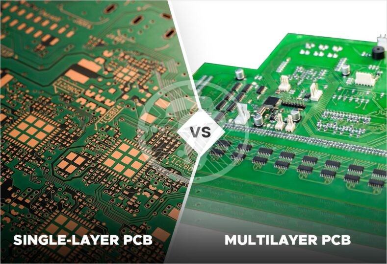
The body of the printed circuit board is made of unbreakable glass or fiberglass with copper foil applied to one or both sides of the glass or fiberglass. Therefore, PCBs made of unbreakable paper-based phenolic resin with bonded copper foil are cheaper and are often used in household appliances.
