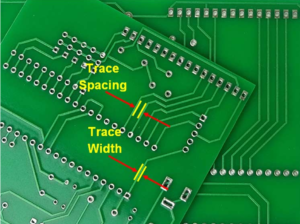
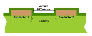
In the usual PCB design, we will encounter various safety clearance issues, such as vias and pads The spacing, the spacing between traces and traces, etc. are all things we should consider. So today we divide these spacing requirements into two categories, one is: electrical safety spacing; the other is: non-electrical safety spacing.
1. The spacing between the wires According to the production capacity of the PCB manufacturer, the spacing between the traces should not be less than 4MIL. The minimum line spacing is also the line-to-line and line-to-pad spacing. So, from the perspective of our production, of course, the bigger the better if conditions permit. The conventional 10MIL is more common.
2. Pad aperture and pad width: According to the PCB manufacturer, if the pad aperture is mechanically drilled, the minimum should not be less than 0.2mm, and if laser drilling is used, the minimum should not be less than 4mil. The aperture tolerance is slightly different depending on the plate. Generally, it can be controlled within 0.05mm. The minimum land width must not be lower than 0.2mm.
3. The distance between the pad and the pad: According to the processing ability of the PCB manufacturer, the distance between the pad and the pad shall not be less than 0.2MM.
4. The distance between the copper skin and the board edge: the distance between the charged copper skin and the PCB board edge is preferably not less than 0.3mm. If it is a large area of copper, it usually needs to be retracted from the board edge, generally Set to 20mil. Under normal circumstances, due to mechanical considerations of the finished circuit board, or to avoid curling or electrical shorts caused by exposed copper on the edge of the board, engineers often shrink large-area copper blocks by 20 mils relative to the edge of the board. The copper skin is not always spread to the edge of the board. There are many ways to deal with this kind of copper shrinkage. For example, draw a keepout layer on the edge of the board, and then set the distance between the copper paving and the keepout.
1. Character width, height and spacing:
For silk screen characters, we generally use conventional values such as 5/30 6/36 MIL, etc. Because when the text is too small, the processed printing will be blurred.
2. The distance from the silk screen to the pad:
Silk printing is not allowed on pads. Because if the silk screen is covered with the pad, the silk screen will not be tinned during the tinning, which will affect the component mounting. Generally, the board factory requires a space of 8mil to be reserved. If it is because some of the PCB board area is very tight, we can barely accept the 4MIL spacing. Then, if the silk screen accidentally covers the pad during design, the board factory will automatically eliminate the part of the silk screen left on the pad during manufacturing to ensure that the pad is tinned. So we need to pay attention.
3. 3D height and horizontal spacing on the mechanical structure:
When mounting the components on the PCB, consider whether there will be conflicts with other mechanical structures in the horizontal direction and the height of the space. Therefore, in the design, it is necessary to fully consider the adaptability of the space structure between the components, and between the finished PCB and the product shell, and reserve a safe distance for each target object.

