High density interconnect PCBs are a way to leave more space on a printed circuit board to increase efficiency and speed up transfer speeds. It’s relatively easy for most aggressive companies using printed circuit boards to understand how this will benefit them.
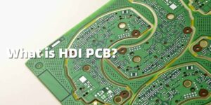
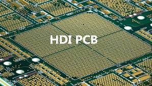
High Density Interconnect HDI PCBs represent one of the fastest growing segments of the printed circuit board market. Due to their higher circuit density, HDI PCB designs can incorporate thinner lines and spaces, smaller through-hole and capture pads, and higher connection pad density. High density PCBs have blind and buried vias and often contain microvias of 0.006 or less in diameter.
Key advantages of HDI PCBs
The evolution of high-density PCB technology has brought unprecedented design freedom and flexibility to engineers. Designers using HDI high-density interconnect methods can now place as many components on either side of the original PCB as needed. Essentially, HDI PCBs provide designers with more space to work with while allowing them to place smaller components together. This means that high density interconnect PCBs ultimately lead to faster signal transfer as well as enhanced signal quality.
HDI PCBs are widely used to reduce the weight and overall size of products, as well as to enhance the electrical performance of devices. High density PCBs are often found in cell phones, touch screen devices, laptops, digital cameras and 4G network communications. HDI PCBs are also prominent in medical devices as well as in various electronic aircraft components. The possibilities for high-density interconnect PCB technology are seemingly endless.
HDI PCB application
HDI PCBs are used in a variety of industries. As mentioned above, you’ll find them in all types of digital devices such as smartphones and tablets, and miniaturization is key to effective product adoption. You’ll also find high-density interconnect PCBs in cars, airplanes, and other vehicles that rely on electronics.
One of the most critical areas where high-density PCBs are making great strides is in the medical field. Medical devices often require small packages with high transfer rates that only HDI PCBs can provide. For example, implants need to be small enough to fit in the body, but any electronics involved in the implant absolutely must effectively allow for high speed signal transmission. Here, HDI PCBs are truly a godsend. HDI PCBs can also be used for other medical devices such as emergency room monitors, CT scans, and more.
No matter what your industry is, you probably already have some ideas about how high-density interconnect PCBs can make the electronics you manufacture or use better – contact us at PCBCart to discuss. We’ll tell you if you’re on the right path and help you determine exactly how beneficial HDI PCBs can be to your industry. Then, you can determine whether to take the next step.
High-quality, high-density PCBs
Specializing in PCB manufacturing for 12 years, Guangzhou Jujin Technology has earned a hard-earned reputation for manufacturing the highest quality PCBs. Our custom PCB manufacturing capabilities allow you to get the highest quality HDI PCBs at competitive prices with no minimum order quantity required. Our team will run manufacturing check designs on your custom PCB files and consult with you to ensure that manufacturing can proceed and that your board will meet your performance requirements. We also have an on-site quality control department to verify that the final product meets your high quality standards.

