


Rigid-Flex PCB design becomes more complex at the stackup stage.
The Rigid-Flex PCB Stackup defines how the rigid and flexible sections function as one structure. In a typical 4-layer rigid-flex design, two rigid FR-4 outer sections support components, while two internal polyimide layers extend through the flex region to provide electrical interconnection and enable 3D folding.
This structure can reduce the number of connectors, save space, and improve reliability. But performance depends on the stackup. Layer arrangement, material selection, and transition-zone design all affect flexibility, signal integrity, and manufacturability.
That is why stackup design is the foundation of a successful rigid-flex PCB.
Why Stackup Matters in Rigid-Flex PCBs
A rigid-flex PCB is not a rigid board with a flex cable attached.
It is a single structure that combines rigid sections for component support, flex sections for bending, and continuous copper layers for electrical connection.
That structure makes stackup design critical.
If the flex region is built like a standard rigid PCB, it can become too stiff for reliable bending. If the design focuses only on flexibility, the rigid sections may not provide enough support for routing, shielding, or signal control.
Rigid-Flex PCB Stackup design is therefore a balance of three factors:
- mechanical flexibility
- electrical performance
- manufacturability
A good stackup is not the most complex one. It is the one that delivers the required performance without adding unnecessary stiffness, risk, or manufacturing difficulty.
The Three Zones Every Designer Should Understand
Every rigid-flex PCB includes three structural regions. If you do not think about them separately, the design tends to be harder to optimize.
1. Rigid Section
The rigid section is the mechanically stable part of the board.
It usually includes:
- FR-4 cores
- prepreg
- copper foil
- plated through-holes
- components, connectors, or shields
This is the area where you mount parts and build the electrical structure that needs stability.
2. Flex Section
The flex section is the bendable portion of the board.
This area commonly uses:
- polyimide dielectric
- flexible copper
- coverlay
- adhesive or adhesiveless bonding materials
The flex section allows the board to bend, fold, or move in a constrained space.
3. Transition Zone
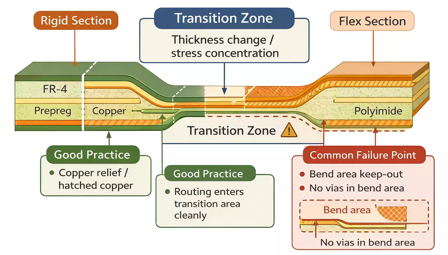
The transition zone sits between the rigid and flex sections.
This is often the most failure-prone part of the design because it combines:
- changing layer structure
- mechanical stress concentration
- copper discontinuities
- local thickness variation
If a rigid-flex board cracks, delaminates, or develops fatigue issues, the transition zone is often where the problem starts.
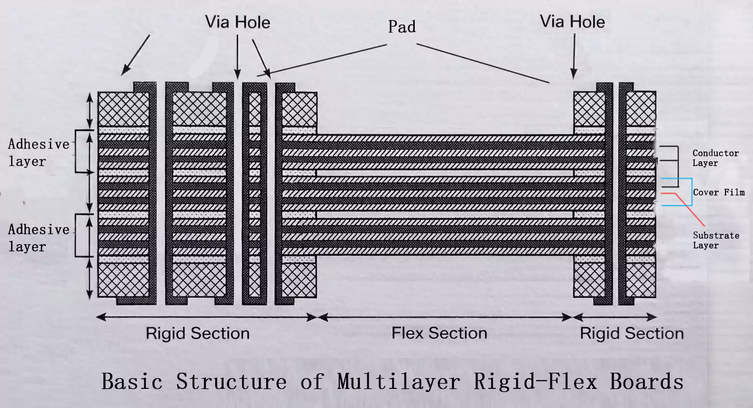
The Basic Materials in a Rigid-Flex Stackup
Rigid-Flex PCB Stackup uses two different material systems in the same product. That is one reason they require more careful planning than standard rigid PCBs.
Rigid Materials
The rigid areas usually rely on familiar multilayer PCB materials, including:
- FR-4 core for structural support
- prepreg for bonding layers during lamination
- copper foil for signal and plane layers
FR-4 remains the most common rigid material because it offers a strong balance of cost, availability, and thermal performance.
Flex Materials
The flex section uses a different material system, usually centered around:
- Polyimide as the flexible dielectric
- copper as the conductor
- coverlay for insulation and protection
Polyimide is widely used because it can tolerate heat while remaining flexible. Copper thickness matters more in flex designs than in rigid ones because it directly influences bendability and fatigue life.
Coverlay vs. Solder Mask
This point is often misunderstood.
In flex sections, coverlay is typically used instead of standard solder mask. Coverlay is designed for bending and long-term protection in flexible circuits. It behaves differently from solder mask and should be treated as part of the flex material stack rather than as a cosmetic surface coating.
Adhesive Systems
Adhesives are another important part of the stackup.
Common options include:
- acrylic-based adhesive systems
- epoxy-based adhesive systems
- adhesiveless constructions
Each has tradeoffs in thickness, thermal behavior, flexibility, and reliability.
Acrylic vs. Adhesiveless: What Is the Difference?
This is one of the most important material choices in rigid-flex design.
Acrylic-Based Constructions
Acrylic adhesive systems are common and well-established. They are often used in mature, widely available flex constructions.
Typical advantages include:
- familiar manufacturing processes
- broad availability
- proven use in many commercial designs
Potential drawbacks may include:
- added thickness
- less favorable thermal behavior in some demanding applications
- more mechanical buildup in tight bend areas
Adhesiveless Constructions
Adhesiveless flex materials remove the separate adhesive layer and typically offer a thinner construction.
They are often chosen when the design needs:
- tighter bend performance
- thinner flex regions
- better thermal stability
- improved performance in more demanding applications
How to Read Rigid-Flex PCB Stackup Language
Rigid-Flex PCB Stackups are often described with shorthand notation that can look confusing at first.
For example:
- 2ML U-1F2R
- 4ML S-2F4R
- 6ML S-2F6R
These labels help describe the number of layers in the flex and rigid portions, as well as whether the construction is symmetrical or unsymmetrical.
Symmetrical Stackups
A symmetrical stackup is mechanically more balanced. In general, it is easier to control stress, thickness distribution, and warpage with a symmetrical construction.
Unsymmetrical Stackups
An unsymmetrical stackup may still be the right solution, especially when the product shape or routing challenge demands it. But it usually requires more deliberate engineering because it introduces more mechanical imbalance.
Common Rigid-Flex PCB Stackup Patterns by Layer Count
Layer count affects both the electrical capability and the mechanical behavior of a rigid-flex PCB.
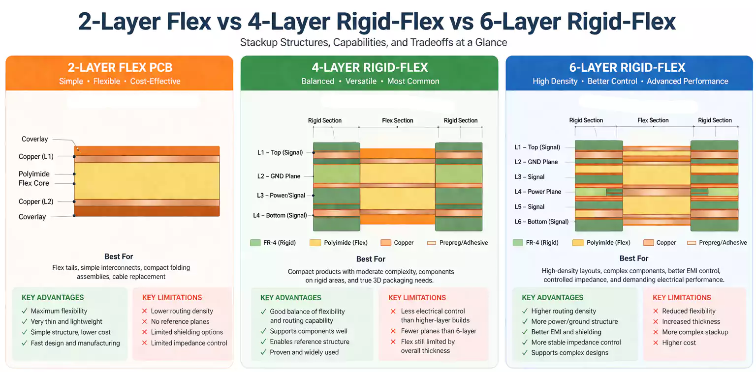
2-Layer Flex PCB Stackup
A 2-layer flex stackup is the simplest and most flexible option.
It is commonly used for flex tails, simple interconnects, compact folding assemblies, and cable replacement. Its main advantages are low profile, high bendability, and structural simplicity.
Its limitations are equally clear. A 2-layer flex design offers lower routing density, limited reference-plane control, fewer shielding options, and less support for controlled impedance in more complex circuits.
4-Layer Rigid-Flex Design
A 4-layer rigid-flex design is often the most practical starting point.
It provides sufficient routing density for many compact products, supports basic reference structures, and enables components more effectively than a simple flex circuit. At the same time, it remains flexible.
For many applications, this is the balance point between mechanical flexibility and electrical functionality.
6-Layer Rigid-Flex Stackup
A 6-layer rigid-flex stackup is typically used when the design requires greater electrical control.
Common reasons to move to 6 layers include higher routing density, more complex component packages, improved power and ground structure, better EMI control, and more stable impedance management.
The tradeoff is reduced flexibility. As more layers extend through the flex region, the structure becomes harder to keep thin and compliant.
8-Layer and 10-Layer Rigid-Flex
Higher-layer-count rigid-flex designs are used when the product demands more electrical complexity.
These stackups are typically selected for dense packaging, high-speed digital systems, expanded plane structure, stronger EMI mitigation, and tighter signal and power integrity requirements.
At that point, the challenge is no longer just building the board. It is maintaining the required flex performance while supporting a much more complex electrical structure.
4-Layer vs. 6-Layer Rigid-Flex: A Practical Comparison
| Routing density | Moderate | Higher |
| Flexibility | Better | Reduced |
| Reference planes | Basic to moderate | Stronger support |
| EMI control | Good for many designs | Better for demanding designs |
| Impedance control | Possible, but limited by structure | Easier to support |
| Manufacturing complexity | Lower | Higher |
| Cost | Lower | Higher |
| Best fit | Compact products with balanced needs | More complex, denser, or higher-speed systems |
What Is an Air-Gap Rigid-Flex Stackup?
Air-gap stackups are one of the more advanced concepts in rigid-flex design.
In a typical multilayer structure, layers in the flex region are bonded together. In an air-gap construction, certain layers are intentionally left unbonded in part of the flex area to allow the structure to move more freely.
Why Use an Air Gap?
Air-gap constructions may be useful when a design needs:
- Improved flex behavior in a multilayer build
- Reduced stiffness in the bend area
- more selective mechanical control
Coverlay, Stiffeners, and Integrated Rigid Sections
These three features are often mentioned together, but they solve different problems.
Coverlay
Coverlay is a flexible protective dielectric used in flex sections. It protects copper while allowing the circuit to bend.
Stiffeners
Stiffeners are local reinforcement features added to flexible areas.
They are commonly used near:
- connectors
- insertion points
- high-stress areas
- handling areas
A stiffener improves local support, but it does not turn a flex section into a full rigid PCB section.
Integrated Rigid Sections
A true rigid-flex design includes rigid areas as part of the actual laminated structure. These regions can support components, plated holes, and multilayer interconnection in ways that a simple stiffener cannot.
How to Optimize a Stackup for Maximum Flexibility
Designers often ask how to make a rigid-flex PCB more flexible. The answer usually starts at the stackup level, not the routing stage.
Here are the most important principles.
Keep the Flex Region as Simple as Possible
Every extra copper layer, dielectric layer, and bonding interface adds stiffness.
Whenever possible:
- Reduce unnecessary copper in bend areas.
- Keep only essential layers in the flex region.
- Avoid overbuilding the flex section.
Use Thin, Appropriate Materials
Material selection directly affects bend behavior.
In many cases, better flexibility comes from:
- thinner flex dielectric
- thinner copper
- adhesiveless materials
- controlled use of coverlay and bonding layers
Limit Abrupt Structural Changes
Sudden stackup changes concentrate stress.
A more reliable design uses:
- gradual transitions
- well-defined rigid-to-flex boundaries
- carefully controlled transition zones
Keep Vias Out of Bend Areas
This is one of the most common rigid-flex design rules for a reason. Vias introduce stress concentration and increase the risk of failure in flexing regions.
Plan the Stackup Before Routing
If routing starts before the stackup is truly defined, the final design often forces unnecessary compromises.
A better workflow is:
- define the rigid and flex regions
- define which layers continue through flex
- define the transition zones
- confirm material system and thickness targets
- then route
Stackup Decisions That Affect Signal Integrity
Rigid-flex stackup is not only about mechanical survival. It also significantly affects electrical performance.
Reference Planes in Rigid Areas
Rigid sections often provide the best place for solid reference planes, controlled return paths, and component grounding.
Impedance Changes in Flex Areas
The flex section has a different dielectric system, which means impedance behavior changes, too.
That means controlled impedance in rigid-flex design must be evaluated with the actual materials and structure in mind. A trace that behaves one way in FR-4 may behave differently in polyimide-based flex.
Layer Count and Electrical Control
As layer count increases, the designer gains more options for:
- shielding
- reference structure
- crossovers
- power distribution
- noise isolation
But these advantages come at the cost of increased mechanical stiffness and fabrication complexity.
Static vs. Dynamic Flexing
Not all flex applications are the same.
Static Flexing
Static flexing means the board is bent during installation or assembly, then remains mostly in place.
This is common in products where the board folds into a compact enclosure once and stays there.
Dynamic Flexing
Dynamic flexing occurs when the flex section repeatedly moves during the product’s service life.
This places much higher demands on:
- copper fatigue resistance
- material system
- bend-area design
- layer structure
- Overall stackup simplicity
Final Thoughts
The best Rigid-Flex PCB Stackup is rarely the most complex one.
It is the one that gives the product the flexibility it needs, the electrical structure it requires, and the reliability the application demands, without adding unnecessary thickness or manufacturing risk.
For many products, that answer will be a 4-layer rigid-flex design. For others, a 6-layer rigid-flex stackup or higher-layer build may be justified by routing density, shielding, or signal integrity goals.
The important thing is to treat stackup as the architectural core of the design, not as an afterthought once layout is already finished.
For teams developing compact, high-density electronics, that discipline is what turns rigid-flex from a clever packaging idea into a dependable manufacturing solution.
FastTurnPCB supports this design approach by focusing on practical rigid-flex manufacturing requirements from the stackup stage onward.
