Prototype PCB Manufacturer
Rapid-Turn Prototype PCB Fabrication Service
As a China-based prototype PCB board manufacturer, we offer lightning-fast PCB prototype fabrication—from single-piece trials to small-volume runs. Upload your Gerber files now for a precision quote in hours.
Service Overview
What Is PCB Prototyping?
PCB prototyping involves quickly producing a small batch of boards from design files before mass production for functional validation, performance testing, and process evaluation. These prototypes let engineers rapidly spot design flaws and optimize layouts, ensuring flawless large‑scale manufacturing.
Why Choose Our PCB Prototype Fabrication Service?
Fast Turnaround
Standard lead time of 5–7 business days; 3‑day expedited delivery for urgent R&D needs.
High-Precision Capability
Minimum line width/spacing of 4 mil; hole sizes down to 0.2 mm; supports multilayer, flex, and HDI boards.
Comprehensive Quality Control
IPC-610 compliant with AOI, ICT, and X-ray inspections—100% coverage to eliminate manufacturing defects.
One-Stop Service
From prototyping and SMT assembly to stencil fabrication and DFM checks, streamlining communication and shortening project cycles.

Product Showcase
Process & Workflow
Design Submission
- Upload Gerber/CAD Files
- Supports Gerber 274X, ODB++, and IPC-2581 formats
- Files auto-archived with a unique project ID
Technical Review
- Manual Assessment Within 2 Hours
- Key checks: minimum line width/spacing, hole diameter, solder-mask openings, and mask clearance
- Optimization suggestions issued and confirmed via email or phone
Prototyping & Fabrication
- Shop Floor Setup: Fully automated CNC drilling and high‑precision copper lamination.
- Process Support: Single-/double-sided, multilayer, flex, and HDI boards
- Strict Environmental Control: Temperature regulation and thorough cleaning prevent contamination and ensure flat, even surfaces
Quality Inspection
- 100% AOI Automatic Optical Inspection: instantly detects opens, shorts, and missing pads
- ICT In-Circuit Testing: covers grid test points to ensure complete signal integrity
- X-ray Layer Inspection: verifies buried/blind vias and lamination quality
Shipping & Support
- Anti-static vacuum packaging with desiccant
- Multiple carriers: EMS, DHL, UPS, all fully trackable
- Tracking number sent within 24 hours of shipment and 7×12 hour online technical support
Capabilities
Capability | Parameter |
---|---|
Layer | Up to 50 Layers |
Max Size | 600 x 500mm |
Thickness | 0.2-7.0mm |
Copper Thickness | 0.33-12 0Z |
Min Line Width/Spacing | 2.5mil/2.5mil |
Min Drill Hole | 6mil |
HoleMin Hole To Line | 5mil |
Impedance Tolerance | +10% or +5% |
Dimension Tolerance | ±0.1mm |
Material |
Shengyi S1000-2, S1141, ITEQ IT180A, Aluminum-Based & Copperbased, Rogers4350B,4003C,3003, RT5880,RT6010,TMM10/10iVT901, DuPont PI, ISOLA FR408HR, 370HR, TU872LK, Megtron 4, Megtron 6 etc. |
Coverlay Opening Size | ≥0.6mm x 0.6mm |
Surface Treatment |
ENIG ENEPIG I-Ag OSP HAL/HAL Lead Free Flash Gold Hard Gold |
Industry Use Cases
Aerospace & Defense Prototype Boards
Applications: Aerospace and defense-grade reliability, multi-layer HDI designs, and strict impedance control. Features: IPC-6012 Class 3, ±5% impedance tolerance, ENIG finish.
Medical Device Prototypes
Applications: Miniature, high‑density circuits for medical devices requiring biocompatible materials and ultra-thin boards. Features: 2.5 mil minimum line width, PI flex substrate, 100% AOI + ICT inspection.
Automotive Electronics Prototyping
Applications: In-vehicle control units and sensor interface boards, with stable operation in high-temperature environments. Features: Heat-resistant 1.6 mm board, 2 oz copper, and vibration-resistant ENEPIG surface finish.
IoT & Consumer Electronics
Applications: Rapid iteration of smart home systems, wearable devices, and consumer electronics. Features: Supports ultra-thin 0.2 mm PCBs, flexible–rigid integration, and one-stop multi-process delivery.
faq
The manufacturing time of PCB prototypes varies due to various factors, including the complexity of the circuit board, the manufacturing plant's production capacity, and order volume.
Generally speaking, simple single or double-sided board prototypes can be manufactured in a few days, while complex multi-layer boards or circuit boards containing special processes such as blind holes and buried holes may require longer time.
To shorten the manufacturing cycle, it is recommended to choose PCB manufacturers with advanced manufacturing equipment and efficient production processes.
Poor circuit: such as open circuit, short circuit, circuit width or spacing not meeting design requirements, etc.
Pad issues: Pad detachment, incorrect pad size, mismatch between pad and component pins, etc.
Drilling problems: aperture deviation, incorrect hole position, poor hole wall quality, etc.
Surface treatment defects: such as uneven coating of solder mask, blurry character printing, insufficient coating thickness, etc.
These issues may be caused by design errors, improper process control during manufacturing, or material quality problems.
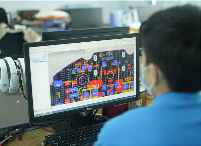
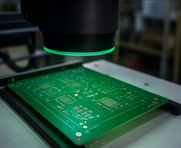
Therefore, a detailed design review should be conducted before manufacturing, reliable manufacturers should be selected, and strict quality control should be implemented during the manufacturing process.
Manufacturing capability: Does the manufacturer have advanced manufacturing equipment and processes to meet your design requirements and production capacity needs.
Quality control: Whether the manufacturer has established a sound quality management system and can provide reliable quality assurance and after-sales service.
Price and delivery time: Compare the prices and delivery times of different manufacturers and choose the manufacturer with high cost-effectiveness.
Technical support: Does the manufacturer provide technical support and solutions, and can they assist in solving problems during the design or manufacturing process.
Electrical performance: The dielectric constant, dielectric loss, resistivity, and other electrical properties of the material should meet the design requirements.
Mechanical strength: The mechanical properties such as bending strength and impact strength of the material should be sufficient to ensure the reliability and durability of the circuit board.
Thermal stability: The material should have good thermal stability and be able to withstand certain temperature changes without deformation or cracking.
Processing performance: The material should be easy to process, such as drilling, etching, electroplating, and other processes should be able to proceed smoothly.
Cost: While ensuring performance, the cost of materials should be considered and materials with high cost-effectiveness should be selected.
Electrical testing: Check the conductivity, insulation resistance, withstand voltage and other electrical performance of the circuit.
Functional testing: Verify whether the circuit board works according to design requirements, including signal transmission, power distribution, and other functions.
Reliability testing: such as thermal cycling testing, wet heat testing, vibration testing, etc., to evaluate the reliability of circuit boards during long-term use.
Appearance inspection: Check the appearance quality of the circuit board, such as solder joint quality, solder mask coating, character printing clarity, etc
Put your parts
into production today
All information and uploads are secure and confidential.