

In rigid-flex PCB design, the bend area is the most failure-prone part of the structure. Bend reliability is primarily controlled by total flex thickness, layer count, and whether the application is static or dynamic. If the bend radius is too small, copper cracking, layer stress, and early interconnect failure become much more likely.
At FastTurn PCB, reliable rigid-flex design starts with the bend radius, bend area layout, and transition zone. These are not separate checks. They are connected design decisions that must be planned together from the beginning.
Key takeaways
- Define the use case first: static and dynamic flexing do not use the same design limits.
- The minimum bend radius should be treated as a design range rather than a single universal value.
- In multilayer flex regions, layer freedom matters more than layer count. Unbonded separation and staggered structures can significantly improve bend reliability.
- Keep vias, plated holes, pads, and components out of the bend zone and away from the rigid-flex transition zone whenever possible.
- Bend-zone failures are usually caused by multiple small decisions, not by a single dramatic mistake.
Bend zones fail for predictable reasons
The rigid sections support components, connectors, and mounting. The flex sections allow folding, movement, and 3D interconnection. The bend zone has to do both jobs at once, which makes it more vulnerable than a normal routing area.
The highest-risk region is not only the bend line itself. It is the bend line plus the transition zone on both sides, where rigid and flex materials meet, coverlay edges change, and local stiffness can spike. Industry guidance commonly treats that transition region as a dedicated control area for layout and fabrication.
Step 1: Define static and dynamic flexing
Before choosing a bend radius or routing pattern, decide how the flex section will be used.
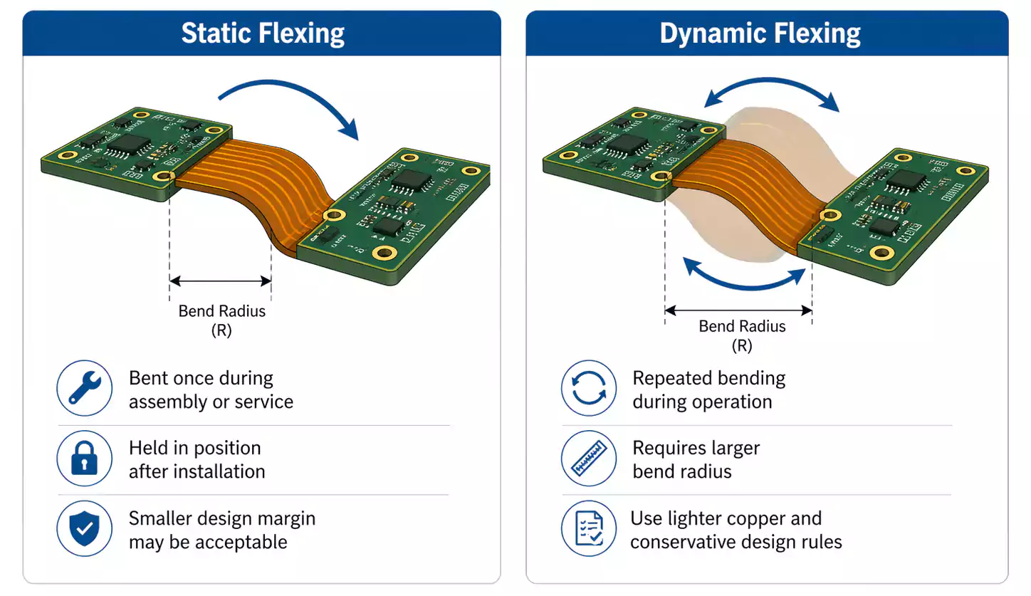
| Static flex | Bent during assembly or service, then held in place | More forgiving mechanically |
| Dynamic flex | Bent repeatedly during normal operation | Requires much more conservative design |
Dynamic applications need tighter control over bend radius, copper thickness, trace geometry, and material choice because fatigue becomes the dominant failure mode.
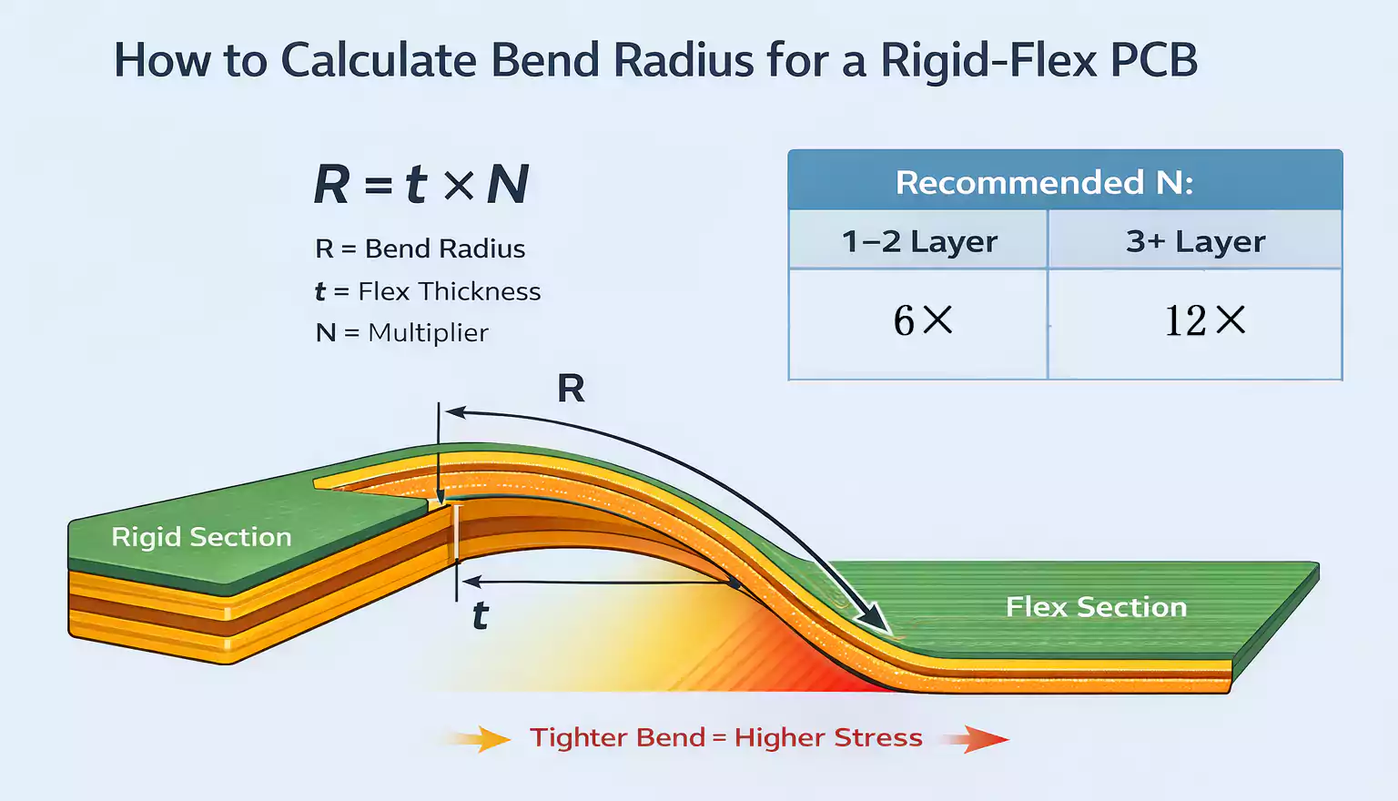
Step 2: Use bend radius as a range, not a fixed rule
Minimum bend radius depends on total flex thickness, layer count, copper weight, and cycle life.
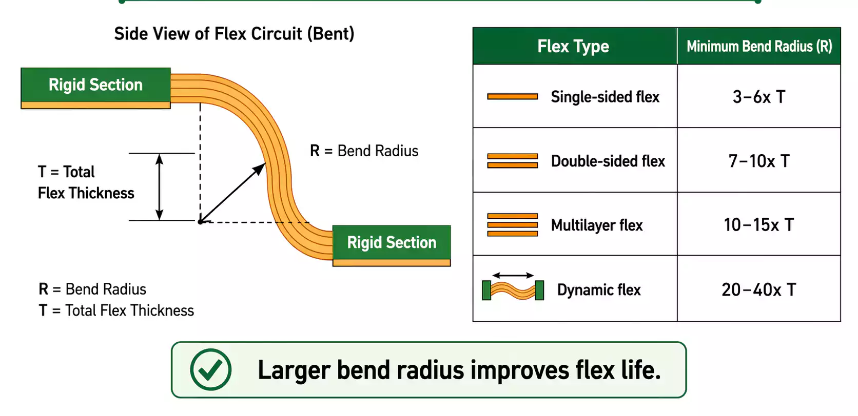
Common starting guidelines
| Single-sided flex | 3–6x total flex thickness |
| Double-sided flex | 7–10x total flex thickness |
| Multilayer flex | 10–15x total flex thickness |
| Dynamic flex | 20–40x total flex thickness |
These are commonly used rule-of-thumb values as starting points.
More conservative production guidance
| Single-layer static flex | 6x thickness |
| Double-layer static flex | 12x thickness |
| Multilayer static flex | 24x thickness |
| High-cycle dynamic flex | Up to 100x thickness |
More conservative design guidelines push radii higher, especially for repeated-flex applications.
What matters most
A larger bend radius improves bend life. Thin materials, fewer layers, and lighter copper also increase durability over time.
The technical source material supports the same logic: when the flex section is long enough, and the film and copper are thin enough, special structural treatment may not be necessary; short bend regions are much harder to make reliable.
Step 3: Give the layers room to move in the bend area
In a bend zone, the real issue is not simply how many layers exist. It is whether those layers can deform without forcing all the strain into the same spots.
The source material notes that unbonded flex-layer separation improves bending performance because the layers can move more independently of one another.
That matters because inner and outer layers do not travel the same path through a bend. If multiple flex layers are forced into the same length in the bend area, the structure tends to wrinkle, strain unevenly, and lose long-term reliability.
Good design principle
Let the layers absorb strain gradually.
Poor design pattern
Force every layer into the same geometry and expect them to bend the same way.
Step 4: Be extra careful with short bend zones
Long flex sections can naturally distribute strain. Short flex sections cannot.
When the bend region is short, there is less room to absorb the mismatch between layers. That is why short bend zones often fail sooner and need more deliberate structural design.
When a bookbinder-style structure helps
For short, high-reliability bend sections, a bookbinder-style structure can improve performance. In that arrangement, the flex layers are made progressively longer from the inside outward, which helps maintain more uniform spacing during bending and reduces wrinkling and localized stress.
Tradeoff
This structure is more difficult and less efficient to manufacture, so it is usually better suited to high-reliability products than to cost-sensitive consumer builds.
Step 5: Choose materials that can actually survive the bend
Material choice sets the ceiling for bend-zone reliability.
The source material emphasizes two core requirements:
- Heat resistance
- Dimensional stability
Material tendencies by application
| High-reliability systems | Thicker polyimide films, often above 50 µm |
| Thin consumer products | Thinner dielectrics, often below 50 µm |
Adhesive system tradeoffs
| Acrylic adhesive | Better bond strength | Lower heat resistance, higher shrinkage |
| Epoxy adhesive | Better thermal resistance | Longer cure, slightly lower bond strength |
| Adhesiveless copper-clad material | Better thermal performance, lower CTE, thinner final build | May require tighter process control |
For repeated flexing, thinner copper is also usually more forgiving than heavier copper. Industry guidance commonly favors lighter copper for dynamic flex applications.
Step 6: Route the bend zone for strain control
Routing in a bend zone should look more like mechanical design than standard PCB routing.
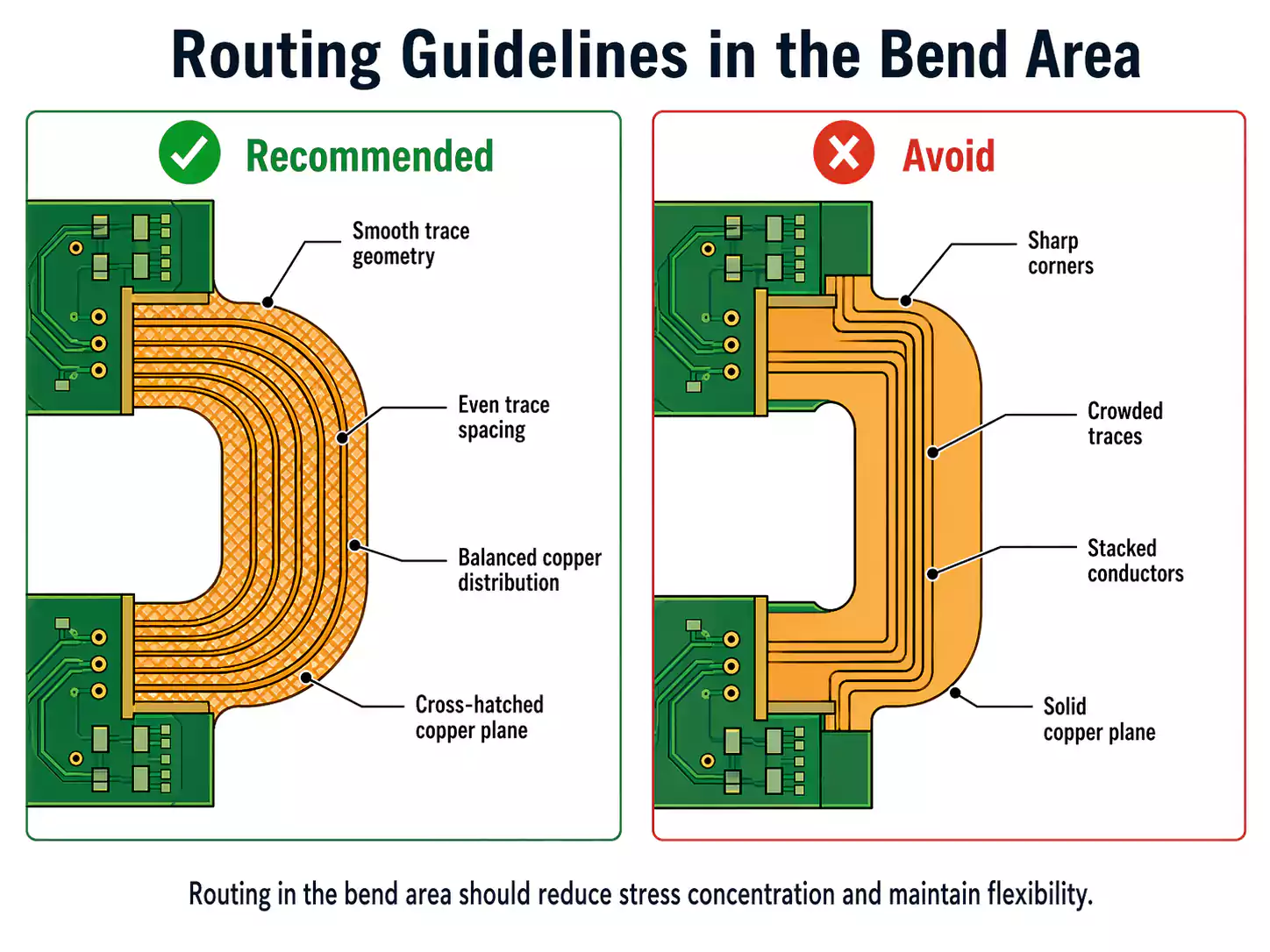
Best practices for routing through a bend
- Use smooth trace shapes.
- Avoid sharp corners and abrupt direction changes.
- Do not crowd too many traces into one narrow band.
- Avoid directly stacking conductors on adjacent layers when possible.
- Keep copper distribution as even as possible across the bend region.
Smooth trace geometry reduces stress concentration and improves flex life.
Why it matters
The goal is not just to get traces across the flex. The goal is to keep the copper from being the first thing to crack in the bend area.
Step 7: Keep rigid features out of the bend zone and transition zone
Vias, plated holes, pads, and components all create local stiffness changes. In a high-strain region, that is exactly what you do not want.
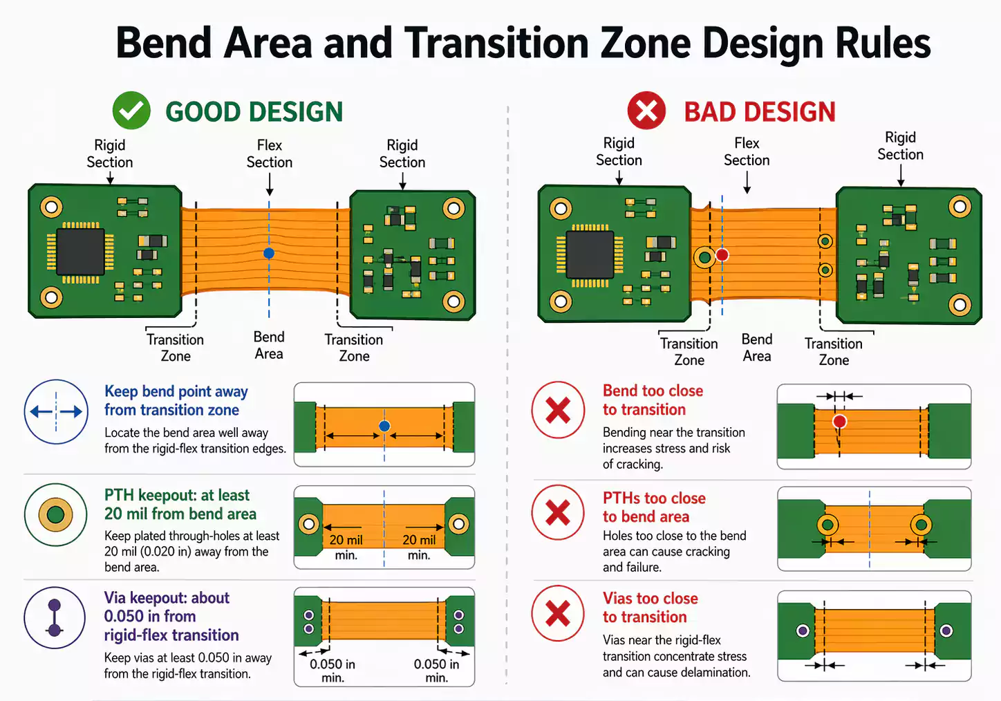
Common keepout guidance
| Plated through-hole to bend area | At least 20 mil |
| Via to rigid-flex transition | About 0.050 in |
| Outer-layer features to transition boundary | About 0.025 in or more |
These are commonly used starting points for DFM review.
Practical rule
Treat the bend zone and the rigid-flex transition zone as intentional keepout regions from the start of layout.
Step 8: Do not assume solid copper is better
A solid copper plane can improve electrical behavior on a rigid board, but in a flex region, it can also make the structure too stiff.
That is why many bend-zone design guidelines prefer cross-hatched copper when a reference plane must be maintained in the flex region.
Common starting pattern
| Hatch line width | 0.015 in |
| Hatch spacing | 0.025 in |
This improves flexibility, but it can also change return-current behavior, impedance stability, and EMI performance. In high-speed designs, the plane pattern should be reviewed as both a mechanical choice and an electrical choice.
Step 9: Fabrication details matter just as much as layout
A bend zone that looks fine in CAD can still fail if the build process does not support it.
The source material describes several important fabrication controls:
- Flex-region conductors are covered with coverlay
- Bonding layers are opened in the flex region to prevent bending.
- Rigid outer sections must be routed back or depth-controlled over the bend area.
- Vacuum lamination and proper pressure support help maintain uniform bonding.
- Pre-baking before lamination, plasma treatment, and drilling helps remove moisture and improve reliability.
Bottom line
A good bend-zone design can still fail if the fabrication flow treats it like a standard rigid PCB.
Step 10: Through-holes near the bend zone raise the risk
If plated interconnects are located near the bend zone, the challenge is no longer only about flexing. Hole reliability becomes part of the problem.
The source material notes that conventional permanganate desmear can damage structures when used with acrylic adhesive systems, whereas plasma etching is generally a better choice for rigid-flex builds.
It also recommends:
- Hole wall copper above 25 µm for high-reliability applications
- In some IPC-related cases, above 35 µm
- Positive etchback around 13 µm to improve plated-hole connection quality
What does that mean in practice?
If holes are close to the bend area, the design must withstand both bending strain and plated-interconnect stress.
Bend-zone priorities change by product type
Not every rigid-flex product needs the same bend strategy.
High-reliability aerospace and industrial builds
These designs usually prioritize long-term stability over maximum density. They often use more conservative geometries, thicker plated holes, and more robust structures.
Industrial and medical HDI builds
These push both density and reliability at the same time, which makes the bend zone harder to design. The source material describes line pitches below 100 µm, hole diameters below 100 µm, and very thin adhesiveless polyimide copper-clad materials in this class.
Consumer electronics
These prioritize thin materials, fewer layers, compact packaging, and low cost. The bend-zone design has to support manufacturability as much as reliability.
FAQ
How do you determine the minimum bend radius in a rigid-flex PCB?
A common starting point is to use total flex thickness as the basis: about 3–6x for single-sided flex, 7–10x for double-sided flex, 10–15x for multilayer flex, and 20–40x for dynamic applications.
What is the difference between static and dynamic flexing?
Static flexing is bent once during assembly or service and then remains in place.
Dynamic flexing, which repeatedly bends during operation, requires a more conservative design.
How much larger should the bend radius be in dynamic applications?
Dynamic applications often require at least 20–40x the flex thickness. Higher-cycle designs may need even larger radii.
Can vias be placed in or near a bend zone?
They should be avoided whenever possible. A common rule is to keep plated-through holes at least 20 mil from the bend area and vias about 0.050 in from the rigid-flex transition.
Why should routing in the bend zone avoid sharp corners?
Smooth trace shapes reduce stress concentration and improve bend life.
Should the bend zone use solid copper or cross-hatched copper?
If a plane is needed in the flex region, cross-hatched copper is often preferred because it reduces stiffness and improves flexibility.
How many times can a flex circuit bend before it fails?
There is no fixed number. Bend life depends on flex type, materials, copper thickness, routing, and bend radius.
What are the most common causes of bend-zone failure?
Common causes include:
fabrication that does not support the flex structure
bend radius that is too small
insufficient layer freedom
vias or components too close to the bend zone
excessive solid copper
unsuitable materials
Final thoughts
A bend zone should not be designed only to survive the first fold. It should be designed to survive the real-life of the product.
That means:
- Define whether the flex is static or dynamic.
- Choose a bend radius that matches the thickness and cycle life.
- Give the layers enough mechanical freedom.
- Keep rigid features out of the flexing region.
- Select materials that support both heat and movement.
- Make sure fabrication supports the flex structure rather than working against it.
The earlier these decisions are made, the easier it is to manufacture the project reliably. At FastTurn PCB, bend-zone reliability starts with that early alignment between design intent and fabrication reality.
