


Rigid-flex PCB design requires more than electrical connectivity. It requires careful control of layer stackup, bend radius, and the transition between rigid and flex sections to prevent mechanical failure.
Most bend-area cracks are not random defects. They are usually caused by a few predictable design mistakes: placing vias or pads too close to the bend area, routing conductors in ways that increase strain, or choosing a bend radius that is too small for the flex thickness. In general, the minimum bend radius is based on the total flex thickness multiplied by an application-dependent factor, with higher ratios required for multilayer and dynamic-flex designs.
A reliable rigid-flex design starts with a few core rules: keep components and vias out of bend zones, route traces perpendicular to the bend axis where possible, use gradual transitions between rigid and flex sections, and design to recognized standards such as IPC-2223. When these mechanical constraints are considered early, rigid-flex boards can deliver the space savings and reliability they are known for.
Quick Answer: Why Do Rigid-Flex PCBs Crack?
Rigid-flex PCBs typically crack because the flex section is forced to bend beyond what its thickness, layer count, and copper structure can safely support. Common causes include a bend radius that is too small, vias and pads placed in or near the bend area, sharp trace geometry, and overly rigid copper patterns in the flexible section.
The 5 DFM Rules at a Glance
| Define the application and stackup first | Flex life depends on motion type, thickness, and layer structure | Overbuilt or underdesigned flex section |
| Calculate bend radius before layout | The bend radius sets the strain level in the flex | Copper cracking, delamination |
| Keep vias, pads, and components out of bend/transition zones | Holes and rigid features create stress concentration | Barrel cracking, pad lifting |
| Route traces for bending | Trace direction and shape affect mechanical fatigue | Trace fractures at corners or narrow transitions |
| Optimize copper and reinforcement features | Copper style, teardrops, and pad geometry affect durability | Early fatigue, poor adhesion, lifted features |
These rules reflect the common guidance repeated across leading flex and rigid-flex design resources.
Why Rigid-Flex PCBs Crack in the Bend Area
At the root level, bend-area failure is a strain problem.
When a rigid-flex PCB bends, the copper and surrounding materials are exposed to tension on one side and compression on the other. If the flex section is too thick, the bend is too tight, or the geometry forces strain into a localized area, the copper can fatigue over time. That fatigue may show up as cracked traces, pad lifting, or delamination near the bend or the rigid-to-flex transition. Siemens and Sierra both emphasize that flex circuits must be designed around mechanical stress from the very beginning.
Static vs. Dynamic Flexing
One of the most important distinctions in rigid-flex design is whether the board bends once or repeatedly.
- Static bend: the board is bent during installation and then remains in place
- Dynamic bend: the board bends repeatedly during product use
That difference drives almost every important design choice. Dynamic applications require much more conservative bend radii and generally place stricter limits on layer count and copper structure.
The Transition Zone Is a High-Risk Area
The rigid-flex transition is not just a visual boundary on the layout. It is a stress-concentration zone where stiffness changes abruptly. That change in mechanical behavior is exactly why features placed too close to the transition are more likely to fail. All Flex specifically advises keeping vias at least 0.050 inch (1.27 mm) away from the flex-to-rigid boundary, and MCB similarly lists a 1 mm minimum distance from vias to the flex area in rigid-flex designs.
DFM Rule #1: Define the Application Type and Stackup Before Layout
One of the most common rigid-flex mistakes happens before routing even begins.
Many failures start because the layout moves forward before the mechanical use case is defined. Before placing traces, the design team should know how the board will bend and how often. They should also determine the maximum thickness of the flex region without exceeding the yield stress. If these questions are not answered early, the design may look fine in CAD but still fail in use.
Why Stackup Matters So Much
In rigid-flex PCB design, stackup does much more than organize layers. It directly affects flexibility, bend life, manufacturability, and strain distribution.
A thicker flex section needs a larger bend radius. More copper layers usually reduce flexibility. Coverlay choices, material construction, and the transition of rigid and flex regions all influence stress during bending. That is why stackup should be a primary design decision, not a secondary detail.
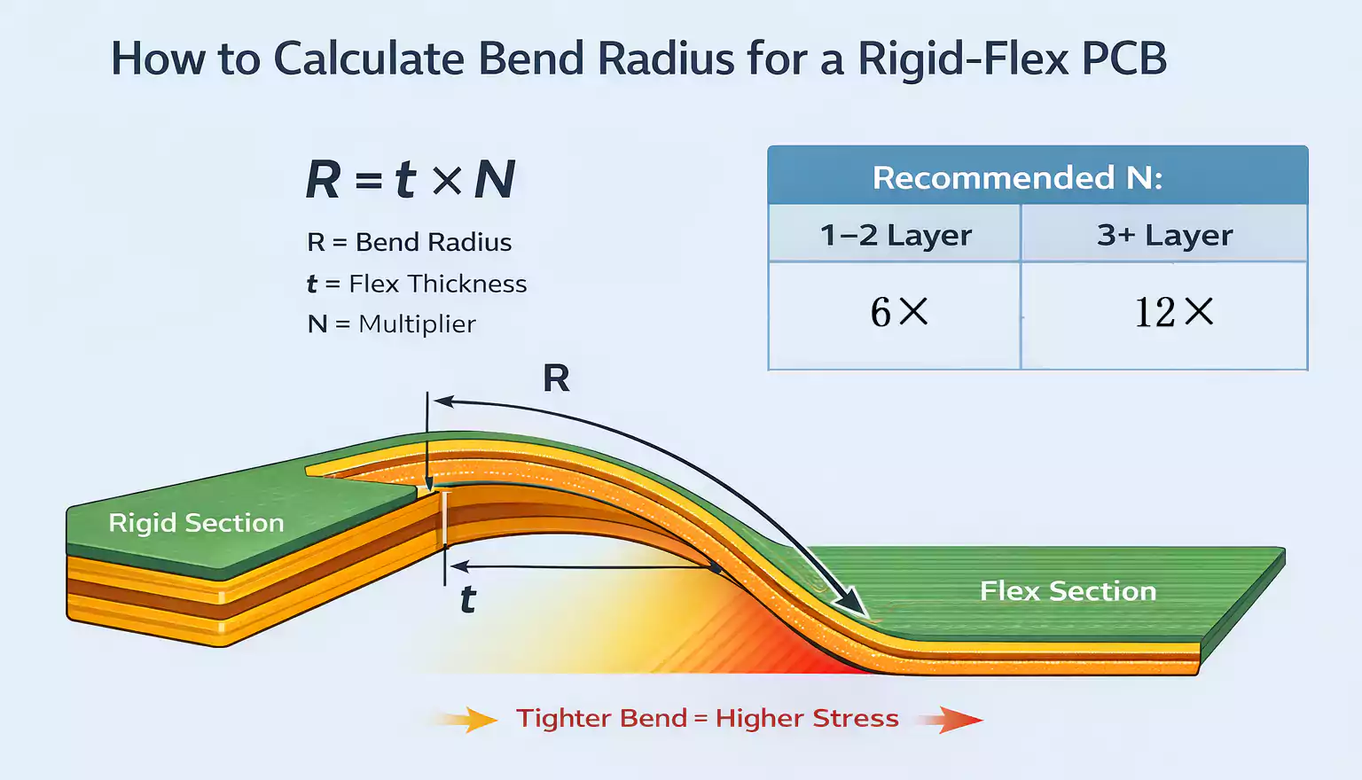
DFM Rule #2: Calculate Bend Radius Before You Route Anything
How to Calculate the Bend Radius for a Rigid-Flex PCB
A practical starting point is:
Minimum bend radius = flex thickness × bend factor
In other words, the thicker the flex section is, the larger the bend radius needs to be.
Some guidelines use this as a simple multiplier. Others express it as a ratio between bend radius and flex thickness. Either way, the principle is the same: bend radius should be based on the structure of the flex region and the way it will be used.
Common Starting Values
Different references show slightly different numbers because they assume different applications.
A common rule of thumb is:
- 1–2 flex layers: at least 6× total flex thickness
- 3+ flex layers: at least 12× total flex thickness
More conservative values are often used for dynamic applications:
- 1 layer, static: 10:1
- 1 layer, dynamic: 100:1
- 2-layer, static: 10:1
- 2-layer, dynamic: 150:1
- Multilayer, static: 20:1
- Multilayer, dynamic: generally not recommended
Why the Numbers Vary
This is where many readers get confused.
These values are not necessarily contradictory. Some are simplified design rules used as quick starting points. Others are more conservative recommendations for dynamic bending and long flex life. The important thing is not to memorize a single number. The important thing is to choose a bend radius based on thickness, layer count, and actual motion.
Example Calculations
A few simple examples help make the concept clearer:
- If the flex section is 0.20 mm thick and you use a 6× rule, the starting bend radius is 1.2 mm.
- If the same section uses a 10:1 rule, the starting bend radius is 2.0 mm.
- If the application is dynamic, the required radius may need to be much larger.
DFM Rule #3: Keep Vias, Pads, and Components Out of Bend and Transition Zones
If bend radius controls how much strain exists, feature placement controls where that strain gets concentrated.
That is why one of the most consistent rigid-flex design rules is to keep vias, plated holes, pads, and components out of the bend area and away from the rigid-flex transition whenever possible.
Why These Features Cause Problems
Features such as vias and pads interrupt the smooth flow of strain through the flex material.
Instead of bending evenly, the structure has to bend around localized rigid geometry. That increases the risk of:
- via barrel cracking
- pad lifting
- copper fracture near the pad entry
- early failure at the rigid-flex interface
Even when the electrical design is correct, these local stress points can still become the first place the board fails.
Keep-Out Priorities
The most effective rules are also the simplest.
Avoid the bend area:
- vias
- plated through-holes
- pads
- components
- abrupt copper widening
Use extra caution near the transition zone:
- Maintain a keep-out distance from the rigid-flex boundary.
- avoid crowding features near rollover edges
- Do not place the bend line directly on the rigid edge.
In rigid-flex layouts, empty space in the right place is often a reliability feature, not wasted area.
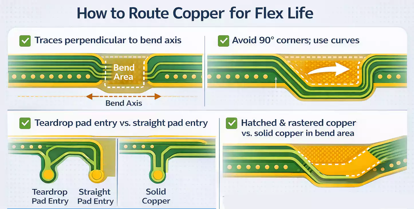
DFM Rule #4: Route Traces for Bending, Not Just for Connectivity
Rigid-flex routing should be designed for motion.
In a standard rigid PCB, routing is usually optimized for density and electrical performance. In a rigid-flex bend region, the goal changes. The layout still has to work electrically, but it also has to survive mechanical strain over time.
One of the most widely accepted practices is to route traces perpendicular to the bend line whenever possible. That orientation spreads strain more evenly across the conductor and usually performs better than routing patterns that concentrate stress into short segments.
Best Practices for Trace Geometry in Flex Areas
A few routing habits make a big difference in flex life:
- route traces perpendicular to the bend axis where possible
- Keep conductors as consistent as possible through the bend area.
- avoid 90-degree corners
- Use curves instead of sharp turns.
- avoid sudden neck-downs
- transition from wide to narrow traces gradually
- Split very wide traces into narrower conductors in the bend area if needed.
Why Sharp Geometry Is Dangerous
A sharp corner is not just a layout style issue. In a flexing structure, it becomes a stress concentrator.
The same is true for abrupt width changes and hard transitions between copper shapes. Smooth curves and gradual geometric changes help distribute strain more evenly, improving durability in the bend region.
DFM Rule #5: Optimize Copper, Pads, and Reinforcement Features for Flex Life
The flex section should not be treated like a normal copper area on a rigid board.
Copper type, copper thickness, pad geometry, and local reinforcement features all influence whether the board bends cleanly or fails early.
Use Copper Structures That Support Flexing
Thinner copper is generally better suited for bend areas than heavier copper. In more demanding applications, copper type matters as well, because different copper structures respond differently to repeated bending.
Large, solid copper areas can also be a problem. Broad, continuous copper makes the flex region stiffer and less compliant. Patterned or reduced copper structures are often used in bend areas to improve flexibility and reduce mechanical stress.
Strengthen Pad-to-Trace Junctions
Pad transitions are a common failure point in flex designs.
Teardrop-shaped pad entries help reduce stress concentration at the point where a narrow trace meets a larger pad. Rounded transitions also improve adhesion and make the structure more mechanically forgiving during bending.
Pad and Annular Ring Sizing Matter More in Flex
Compared with rigid-only boards, flex and rigid-flex designs often benefit from more generous pad and annular-ring geometries.
That added margin can improve adhesion, reduce local stress, and make the design more tolerant of handling and repeated motion.
Use Stiffeners Strategically
Stiffeners are not there to make the entire board rigid.
They are used to reinforce specific areas, such as connector zones, mounting areas, or assembly-sensitive regions, while keeping the actual bend area free to flex as intended. Used correctly, stiffeners improve support without interfering with flex performance.
Common Rigid-Flex Design Mistakes That Lead to Cracks
Watch out for these failure-triggering mistakes:
- choosing layer count before defining motion type
- using a bend radius based only on enclosure space
- routing sharp corners through the bend area
- placing vias near the rigid-flex boundary
- putting pads or plated holes into the bend zone
- using copper structures that make the flex section too stiff
- Treating the transition zone like an ordinary board edge
If a rigid-flex PCB cracks, the root cause is often one of those decisions — or several of them combined.
Final Takeaway
Rigid-flex PCB reliability is determined early in the design stage, not after fabrication.
The most effective way to prevent bend-area failure is to control the fundamentals: define the application, build the right stackup, calculate bend radius early, keep vias and pads out of bend-sensitive regions, and use routing and copper patterns that reduce mechanical stress. These are the design decisions that have the greatest impact on long-term flex reliability.
At FastTurnPCB, we view rigid-flex design as a combined mechanical, electrical, and manufacturing challenge — because that is what reliable performance demands.
