

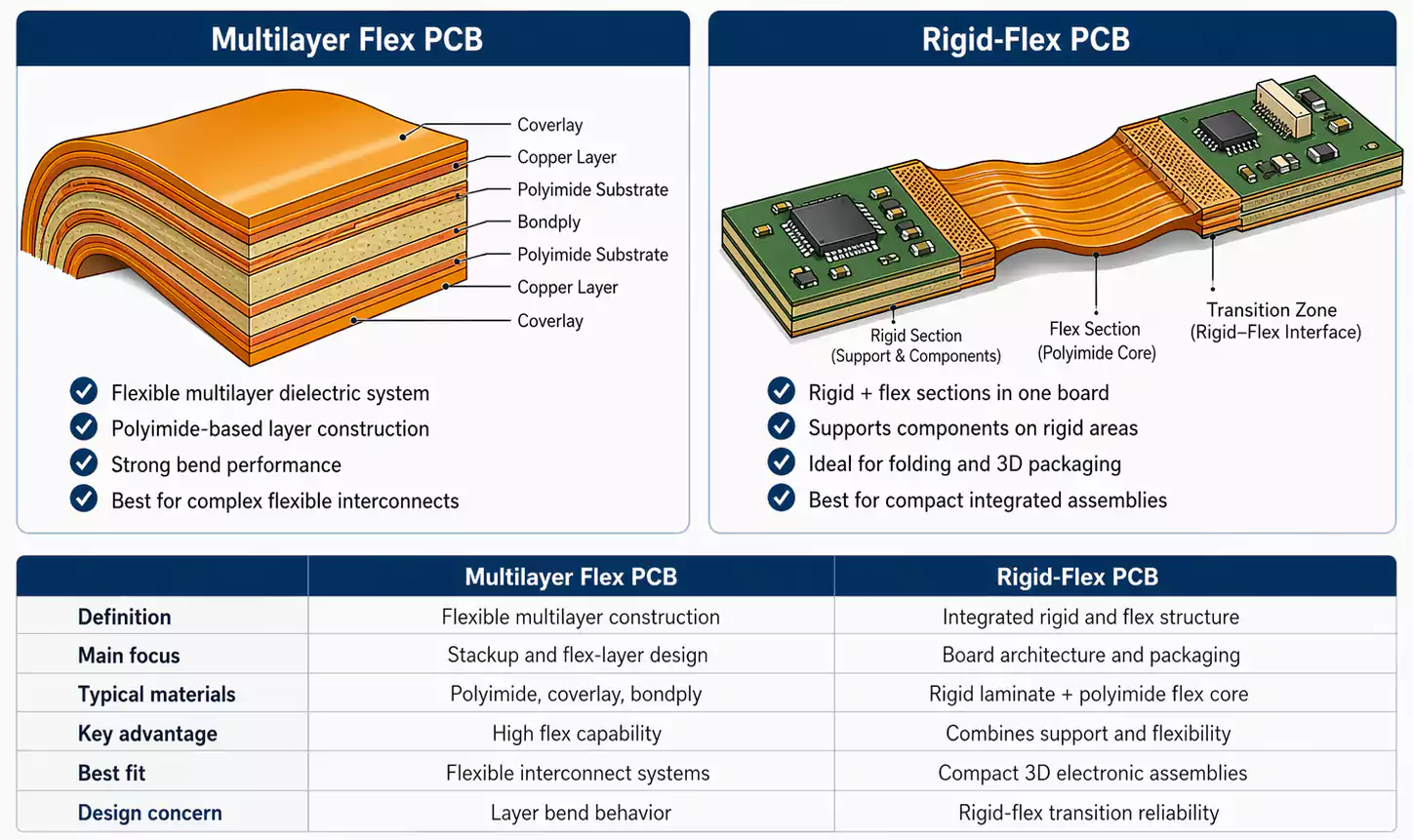
Multilayer Flex PCB vs. Rigid-Flex PCB are closely related, but they are not the same.
A rigid-flex PCB combines rigid and flexible sections in one integrated structure. A multilayer flex PCB refers to a multilayer construction based on flexible dielectric materials.
In simple terms, one describes the structural design of the board, while the other describes the multilayer flexible build.
Quick answer
- A rigid-flex PCB is defined by its combination of rigid and flex regions.
- A multilayer flex PCB is defined more by its multilayer flexible dielectric construction.
In real products, the two can overlap.
Why These Two Terms Are Often Confused
The confusion comes from the way the technology developed.
Rigid-flex structures were originally used in high-reliability electronics, especially aerospace, where designers needed dependable routing in very limited space. In some complex systems, these constructions exceeded 30 conductor layers. Later, consumer electronics pushed the technology in a different direction, with greater emphasis on thinner packages, higher density, and lower cost for products such as mobile phones and digital cameras.
As a result, similar technologies are often described from different perspectives. Sometimes the focus is on the combination of rigid and flexible sections. In other cases, the focus is on the multilayer flexible dielectric construction itself.
Definitions First: These Are Not Strict Opposites
A rigid-flex PCB is an interconnect structure that combines rigid sections and flexible sections in one board. The rigid areas provide component support and mechanical stability, while the flex areas allow bending, folding, or three-dimensional routing.
A multilayer flex PCB is better understood as a multilayer construction built around flexible dielectric materials rather than conventional glass-epoxy rigid materials. In that sense, the term refers more to the material stackup and the organization of flexible layers.
These are not two completely separate categories. In practice, one design may be a rigid-flex PCB from a structural standpoint while also fitting within the broader discussion of multilayer flex construction from a materials standpoint.
Side-by-side comparison
| Main emphasis | Flexible dielectric stackup | Combined rigid and flex structure |
| Best understood as | A multilayer flexible material system | A board architecture with rigid and flex regions |
| Design focus | Layer construction, flex behavior, bend performance | Mechanical integration, rigid/flex transition, packaging |
| Typical discussion topics | Polyimide, adhesiveless materials, coverlay, flex-layer separation | Rigid sections, flex sections, lamination, routing, controlled-depth removal |
| Can the two overlap? | Yes | Yes |
Structural Difference: Board Architecture vs. Flex Layer Construction
The structural difference starts with design intent.
A rigid-flex PCB is primarily about how rigid and flexible sections work together in one product. The rigid areas typically support components, connectors, and mounting features. The flexible areas connect those rigid sections and allow the board to bend or fold within the final assembly.
In many cases, the main challenge is not layer count alone. It is how the rigid and flex sections are arranged, how the bend zones transition, and how the finished board fits into the product enclosure.
A multilayer flex PCB places more emphasis on how the flexible layers themselves are constructed.
For example, multilayer flex designs may use an unbonded flex-layer separation structure to improve bend performance. When flexible layers are tightly bonded together, strain can build up during bending. When the layers have more freedom to move, that strain can be distributed more evenly. In high-reliability applications, this type of construction can support structures with more than 30 layers.
One important point is easy to miss: a higher layer count does not automatically mean a higher-density design.
In aerospace and other high-reliability applications, designers may intentionally avoid fine lines and microvias. Instead, they may use wider trace and space rules, larger plated through-holes, and thicker hole-wall copper because long-term reliability matters more than aggressive miniaturization.
Common rigid-flex form factors
- Folded structures
- Flying-tail structures
- Bookbinder-style structures
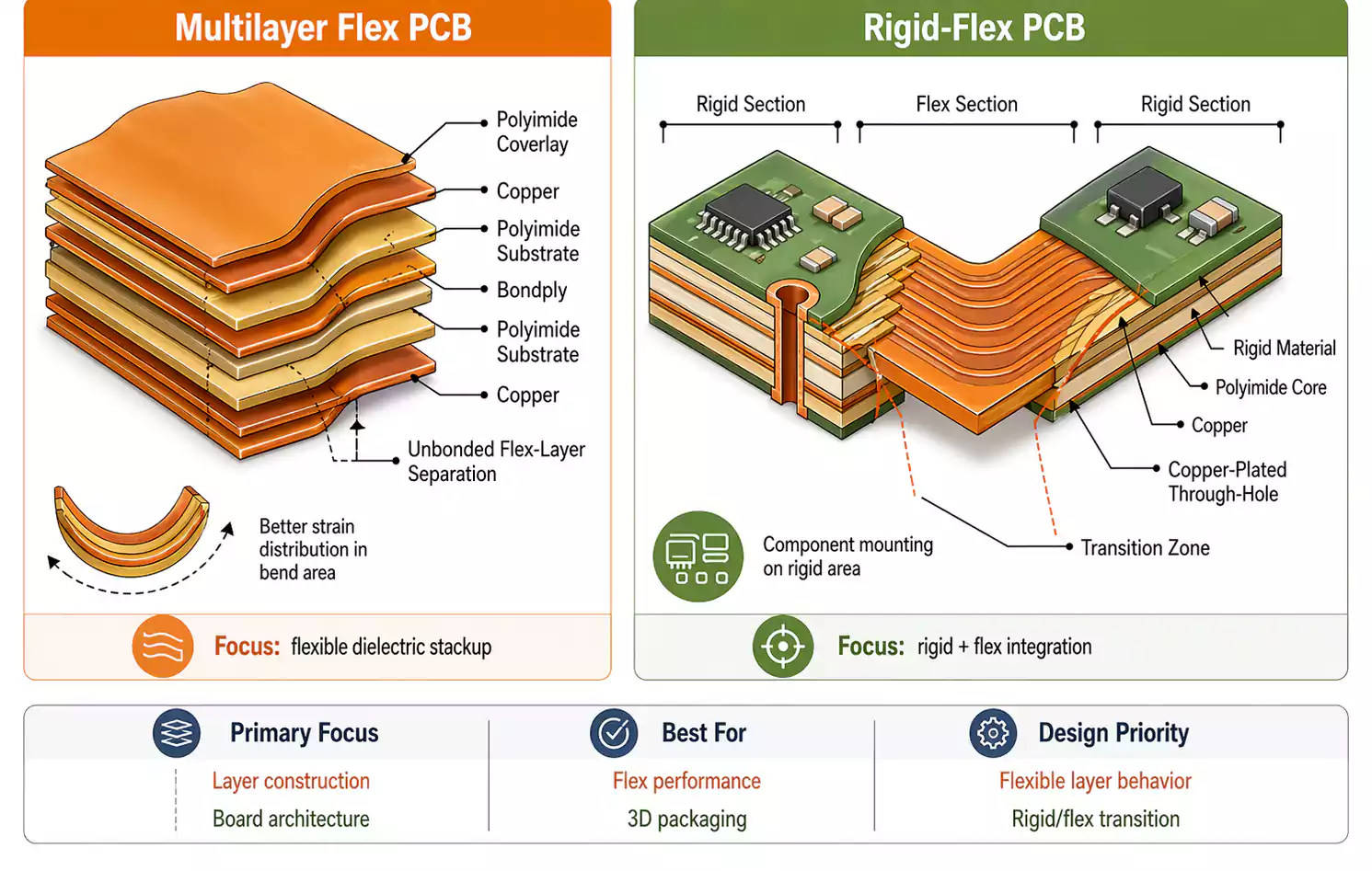
Material Difference: Polyimide, Adhesiveless Copper Clad, Adhesives, and Coverlay
The material system is where the multilayer flex perspective becomes especially important.
These constructions require materials with strong heat resistance and good dimensional stability during processing. In high-reliability applications such as military and aerospace electronics, thicker polyimide film is typically preferred, usually above 50 μm, because it offers better stability and durability. Consumer electronics generally move in the opposite direction, favoring thinner materials, often below 50 μm, to reduce thickness and support smaller form factors.
Adhesive choice also affects the performance balance.
Acrylic adhesives generally offer stronger bonding, but they tend to have lower heat resistance and higher shrinkage.
Epoxy adhesives generally provide better heat resistance, but they usually require longer cure time and may offer slightly lower bond strength.
Adhesiveless copper clad materials are often a major advantage in both rigid-flex and multilayer flex constructions because they can provide:
- Better heat resistance
- Lower thermal expansion
- Reduced final board thickness
Thermoplastic polyimide coverlay and bondply systems have also improved significantly. They can be thinner, more reliable, and more effective at reducing drill smear. The tradeoff is that they may require processing temperatures above 300°C, which increases the demands on equipment and process control.
Manufacturing Difference: Why Rigid-Flex Is More Difficult to Build
Rigid-flex fabrication is more complex because it combines rigid-board and flex-circuit processing in a single build.
A qualified manufacturer must control not only multilayer lamination, drilling, plating, and outer-layer processing, but also flex-specific requirements such as bend-area protection, coverlay handling, controlled-depth rigid removal, and dimensional stability during lamination.
A typical process starts with double-sided flex copper clad material. Circuit patterns are formed by etching, the flex regions are protected with coverlay, and the multilayer flex sections are bonded with bondply opened in the bend area. Rigid outer sections are then added with rigid copper-clad material.
The rigid outer layers may then be machined by CNC routing, punching, or laser processing to remove rigid material from the flex region before final bonding. If routed cavities are used, the flex area may also require press support during lamination. Vacuum lamination and prebaking are commonly used to improve process stability.
Why manufacturing becomes more challenging
- Rigid and flex materials respond differently during lamination
- Bend areas require special protection
- Moisture control becomes more important
- Dimensional compensation is more critical
- Final shaping and forming are more complex than in standard rigid boards
Reliability Difference: Through-Holes, Desmear, Copper Thickness, and Bend-Zone Design
Reliability is where the differences become more significant.
When plated through-holes are used in flexible layers, drilling and hole-processing parameters cannot be copied from standard rigid PCB processes. They must be matched to the specific material system and structure. Prebaking before drilling is especially important for the reliability of plated holes.
Desmear is a key factor. Potassium permanganate is common in rigid PCB processing, but with acrylic adhesive systems, it can cause swelling and reduce hole reliability. For that reason, plasma etching is often preferred for rigid-flex structures. Polyimide-based adhesive systems can also reduce desmear-related issues, although they typically require higher lamination temperatures and more specialized processing.
Hole-wall copper requirements also vary by application. Aerospace and industrial electronics usually require higher plated-hole reliability, with recommended hole-wall copper thickness above 25 μm. In some IPC6013C-related cases, the requirement can exceed 35 μm. Consumer designs may use thinner plated copper to reduce thickness and cost, but reliability still has to meet the application target.
Positive etchback also plays an important role. A depth of about 13 μm is commonly recommended. It helps improve plated-hole reliability by etching adhesive and polyimide layers without attacking the metal, while also cleaning the metal surface and improving copper connection quality.
Why Bookbinder and Flex-Layer Separation Structures Matter
In multilayer flex regions, the key issue is not just whether the board can bend. It is whether each layer bends under compatible strain.
If multiple flex layers are designed with the same length through the bend region, bend performance can suffer. Each layer experiences a different bend radius, so the inner and outer layers do not naturally require the same length during bending. Equal-length layers can lead to wrinkling, uneven spacing, and localized stress.
When the bend length is long enough and the films and copper foils are thin enough, this problem becomes less severe. In those cases, an unbonded flex-layer separation structure can improve bending behavior by allowing more freedom between layers.
When the bend area is short and higher reliability is required, a bookbinder structure is often the better solution. In that design, the flexible layers are given progressively increasing lengths from the inner layer to the outer layer within the bend zone. That helps maintain more uniform spacing and reduces wrinkling during bending.
Bookbinder structure: pros and cons
Pros
- Better bend reliability in short flex regions
- More uniform spacing between layers
- Lower risk of wrinkling and localized stress
Cons
- Requires special tooling and equipment
- Reduces manufacturing efficiency
- Not ideal for cost-sensitive consumer products
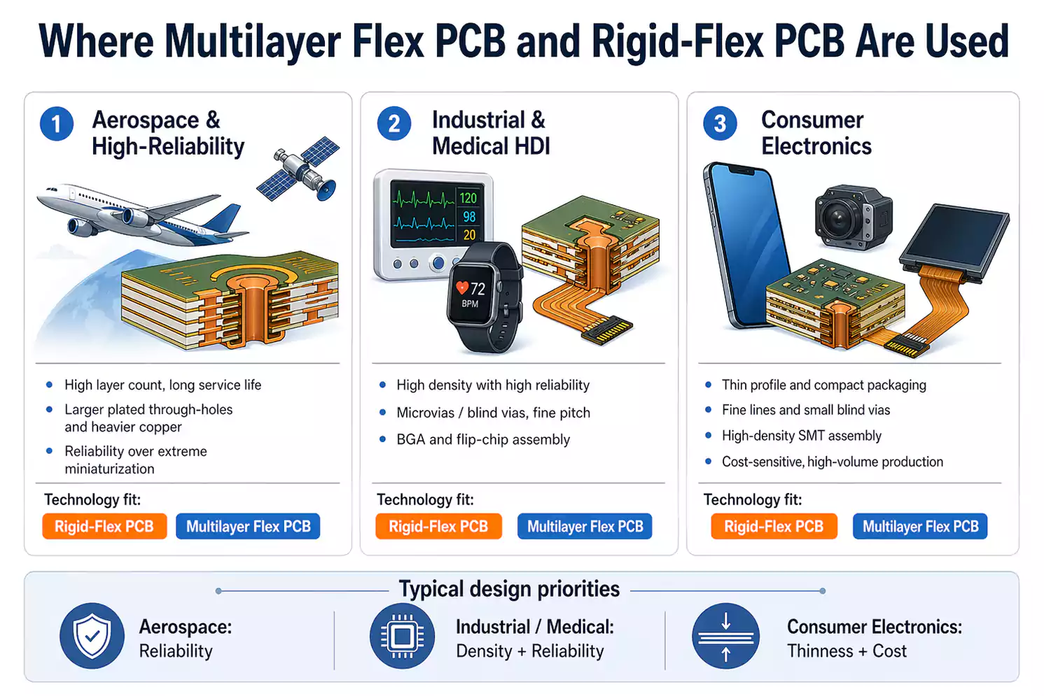
Application Difference: Aerospace, Industrial and Medical HDI, and Consumer Electronics
The application context makes the distinction much clearer.
Aerospace and other high-reliability systems
In aerospace and other high-reliability environments, the priority is dependable routing in limited space, long service life, and strong interconnect reliability.
These designs may use very high layer counts, but they do not necessarily aim for the smallest lines or vias. Larger plated through-holes, wider trace and space rules, and heavier copper are often preferred because long-term reliability matters more than aggressive miniaturization.
Industrial and medical HDI rigid-flex
Industrial and medical applications increasingly combine high density with high reliability.
In these designs, line pitch may be below 100 μm and via diameter below 100 μm. They may use 25 μm or thinner adhesiveless thin-copper polyimide materials, often with copper thickness around 18 μm or less, together with laser-drilled microvias and blind vias. Assembly methods may also include BGA soldering and flip-chip bonding.
Consumer electronics
Consumer electronics follow a different optimization path.
Phones, digital cameras, and display modules need high density, compact packaging, and tight cost control. These products may use line widths below 75 μm, blind vias below 150 μm, and high-density SMT assembly. Many small ICs are mounted on the rigid sections, while the flexible sections connect displays, cameras, or secondary modules.
Consumer-focused designs also tend to:
- Use thinner materials to reduce total thickness
- Allow plated-hole copper below 15 μm when reliability requirements permit
- Replace some glass-epoxy outer material with polyimide film or adhesiveless copper clad
- Keep total conductor layers at 10 or fewer
- Minimize board size and use compact rectangular outlines to improve material utilization and manufacturing efficiency
When to Use Multilayer Flex PCB vs. Rigid-Flex PCB
Use rigid-flex PCB when the discussion is mainly about:
- Integration of rigid and flex regions
- Mechanical packaging
- Folding and 3D assembly
- Transition-zone design
- Manufacturing complexity in hybrid rigid/flex structures
Use multilayer flex PCB when the discussion is mainly about:
- Flexible dielectric stackup
- Polyimide-based multilayer construction
- Layer separation for bend performance
- Material systems such as adhesiveless copper clad, coverlay, and bondply
- Flexible-layer behavior in bending and reliability
Final takeaway
The difference between a multilayer flex PCB and a rigid-flex PCB is not just terminology. It reflects two different design perspectives.
A multilayer flex PCB is defined primarily by its flexible multilayer dielectric construction. A rigid-flex PCB is defined as a board that integrates rigid and flexible sections. In many designs, those distinctions overlap, but the design intent is not the same.
The right term usually becomes clear once the engineering priorities are clear: stackup, bend performance, packaging, reliability, thickness, or manufacturability.
