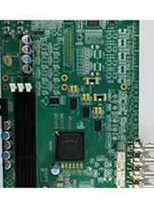


Multi layer Boards
Multilayer 4-50L≥$140/㎡Rigid Flex PCB
5days Delivery≥$135/㎡BOM Procurement
100% original
≥$50/sample
PCB Assembly
Full Turn-Key PCB Assembly
2-4 days Delivery
ABOUT Fast Turn PCB
FAST TURN PCB founded in 2015Y, We have one PCB factory and one PCB assembly factory ,have about 350 employees, We Focus on PCB & PCBA Turnkey solution, Good at small & medium-sized volume, quick turn delivery, we committed to Provide high reliability products to our customer .80% of our products are sold to Europe and America,20% are sold to Asia and domestic, widely used in medical,industrial control,Telecom communication and semiconductor etc.
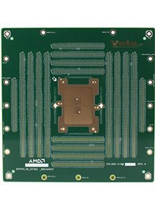
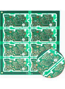
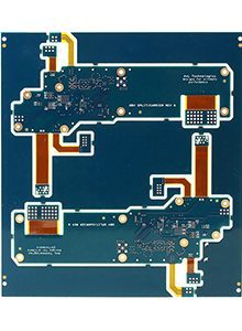
PCB factory Good at multi-layer PCB (4-50 layers), HDI blind & buried board, High frequency material board, Rigid-flex board, certificated by ISO 9001, UL(E520899), Rohs & Reach. Every pcb board will do 100% inner and outer layer AOI, E-test, via hole wall test etc.
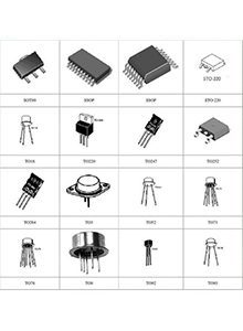
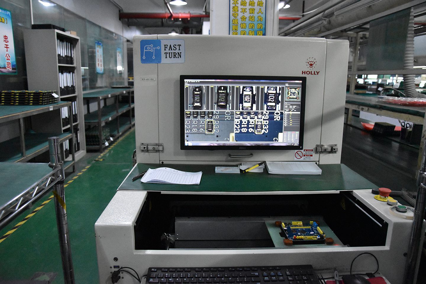
PCBA factory owns capability on BGA, QFN, 0201, 01005; has Quality control equipment like SPI system, AOI, first-piece inspection, X-Ray and so on.
Our Target is to provide “Reliable Quality, Quick Delivery, Professional Service and Fair Pricing”.
PCB Manufacturing,PCB Assembly, Circuit Maker-Fast Turn PCb
Are you looking for a high-quality and full-range PCB fabrication, PCB assembly, and components sourcing services? Then, Fast Turn PCB is here to provide your needs at affordable rates. Yes, you read it right! Our company has been in the industry for many years, guaranteeing the best products and services you will surely love!
Who We Are
A renowned manufacturer in China, Fast Turn PCB is a one stop shop that can provide everything your company needs as far as PCB products and services are concerned. Our company values our customers and thereby never fails to meet your standards and needs.
Our Advantage
Multi-layers 4-10 layers Expedited 2-3 days delivery
HDI PCB Rush Service 5-7 Days
SMT Prototype Rush Service 1-3 Days
Component Purchase Insure parts is original
Difficuit board We have team Work for it
PCB Design 15 years layout 50+ design team
Multi-layers 4-10 layers Expedited 2-3 days delivery
HDI PCB rush service 5-7 Days
SMT prototype rush service 1-3 Days
Ensure that component procurement is original
Difficuit board we have specialized team work for it
PCB design 15 years layout 50+ design team
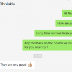
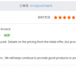
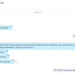
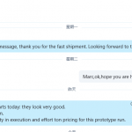
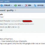
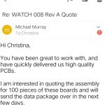
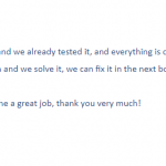
Customer Testimonials






News
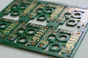
Advantages of thick copper PCB board
Thick copper PCB board refers to a printed circuit board that uses thick copper foil as a conductive material. Compared with ordinary PCBs, thick copper PCBs have higher conductivity and mechanical strength, which can meet the requirements of high current, high voltage, and high mechanical stress. 1) Good thermal conductivity Thick copper PCB circuit boards can effectively dissipate heat and prevent circuit board overheating. Compared to conventional circuit boards, thick copper PCB circuit boards have a thicker thickness and higher copper foil thickness, which can better conduct heat and ensure the stable operation of electronic devices. 2) Improving the reliability of electronic components It can improve the reliability of electronic components. The thick copper layer of a thick copper PCB circuit board can provide better current carrying capacity, reducing the possibility of burning and heat concentration on the circuit board. 3) Enhance the mechanical strength of circuit boards Due to the thickness of the copper layer, it has high mechanical strength. In some demanding environments, such as high vibration and high impact applications, the use of thick copper PCB circuit boards can improve the circuit board’s resistance to vibration and impact, avoiding damage to electronic components caused by mechanical stress.
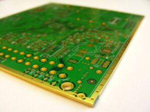
What are each layer in a PCB circuit? What is its purpose?
In the field of electronic engineering, printed circuit boards (PCBs) are indispensable components that carry the connections and communication between electronic components. PCBs are not single-layer structures, but are composed of multiple layers, each with its specific functions and roles. Let’s talk about them together. 1. Mechanical layer Definition: The mechanical layer represents the overall appearance and size of the PCB board. Function: It defines the boundaries, dimensions, assembly instructions, and other information related to mechanical characteristics of the circuit board. Usage precautions: The mechanical layer is often output and displayed together with other layers, but should not be used for electrical wiring. 2. Keep Out Layer Definition: This layer defines the areas on the PCB board that allow for wiring or placement of components. Function: By drawing enclosed areas, boundaries are set for automatic layout and routing to ensure the effectiveness of circuit design. Usage precautions: The wiring layer should not be confused with the mechanical layer, and its boundaries define the scope of electrical wiring. 3. Signal Layer Definition: The signal layer is the area on a PCB board used for arranging wires, including the top layer, bottom layer, and middle layers. Function: The top and bottom layers
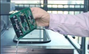
Four factors affecting the stability of PCBA cleaning process
For a considerable period of time, the industry’s understanding of cleaning processes was not sufficient. Mainly because in the past, the assembly density of PCBA was relatively low, and the adverse effects of pollutants such as flux residue on electrical performance were not easily detected. Nowadays, with the development of miniaturization in the design of PCBA, the device size and spacing between devices have become smaller. Failure faults such as short circuits and electrochemical migration caused by small particle residues have attracted widespread attention. In order to adapt to market trends and improve product reliability, more and more SMT manufacturers are embarking on a journey of learning about cleaning processes. The cleaning process is the process of combining the static cleaning force of the cleaning agent with the dynamic cleaning force of the cleaning equipment to ultimately remove pollutants. PCBA cleaning is divided into two stages: SMT and THT. By cleaning, the accumulation of surface pollutants during the processing of the product can be removed, reducing the risk of surface contamination and reliability. In the electronic manufacturing and semiconductor processing industries, it is crucial to choose the right cleaning agent and appropriate cleaning equipment. The factors that affect the stability

8 Various Factors Influencing PCB Board Prices
1: Materials used for PCB Taking ordinary double-sided boards as an example, the board material generally includes FR4, with thicknesses ranging from 0.2mm to 3.0mm and copper thicknesses ranging from 0.5oz to 3oz, which creates a huge price difference in terms of materials; In terms of solder mask ink, there is also a certain price difference between ordinary thermosetting oil and photosensitive green oil. 2: Surface treatment process of PCB Common processes include OSP (antioxidant), lead based tin spraying, lead-free tin spraying (environmentally friendly), gold plating, gold deposition, and some combination processes, etc. Different processes have differences in price. 3: Difficulty in PCB design requirements There are 1000 holes on both types of circuit boards. If the hole diameter of one board is greater than 0.2mm and the hole diameter of the other board is less than 0.2mm, different drilling costs will be formed; If the other two types of circuit boards are the same, but the line width and distance are different, one is greater than 4mil and the other is less than 4mil, it will also affect production costs; Secondly, there are also some unconventional board designs that require additional costs, such as different requirements such as half

Why choose one-stop PCB Assembly services
Electronics manufacturers need a dependable partner to supply the electronic chip that goes into all our smart electronic gadgets. Whether it’s a luxury car or smartwatch, a remote-controlled child’s toy or a glucose monitoring kit at your local health store, the crucial printed circuit board (PCB) is an essential component. Manufacturing a PCB involves a series of complex steps: printing and storing circuit boards, procuring electronic components, assembly, and testing to ensure functionality to specifications. Traditionally, OEMs used a multi-vendor, multi-partner approach to PCB sourcing, manufacturing, assembly, and testing. However, this method was too cumbersome, slow, expensive and error-prone. As a result, the demand for ready-to-use PCBs snowballed, and one-stop PCB assembly services became the preferred choice for electronics manufacturers and designers. The importance of a one-stop PCB assembly services provider End-to-end service providers give OEMs a competitive edge. They can turn their ideas into efficient electronics products, get them out into the market before their competition, and achieve early monetization. When working with a one-stop PCBA (printed circuit board assembly) service provider, the same vendor sources components and assembles the PCB. Maintaining a single point of contact for the entire manufacturing process eases communication in case of any problems,
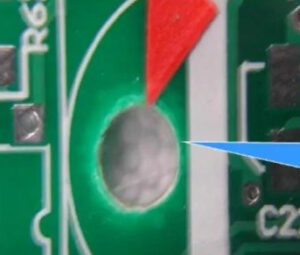
Analysis of the causes and avoidance measures for 9 major defects in PCB boards
1. Poor substrate and leakage of the bottom plate may cause scratches during transportation, resulting in circuit gaps. Easy to affect the impedance of product wiring. Standardize homework and strengthen control. 2. Poor substrate, localized whitening, improper mechanical impact on the board, or infiltration of fluorinated chemicals into the local board, resulting in etching of the woven points of fiberglass cloth. Electrical connections that may affect appearance and signal. High Tg board is required; Minimize or minimize excessive vibration during machining; Choose the appropriate tin and lead removal solution and operating process. 3. Poor substrate with exposed patterns, caused by low resin content or high fluidity of the bonding film, and excessive adhesive flow during lamination; During lamination, the temperature rises and pressure rises too quickly, and the high pressure is applied too early, resulting in too much glue flow. Impact: Causing a decrease in the insulation performance of the substrate, seriously affecting the quality of the PCB board. Avoidance: The method of “surface material” and “inner material” can be used to increase the resin content of the surface material appropriately and adjust the corresponding technical parameters such as GT and RF%. The product should have sufficient curing temperature

