

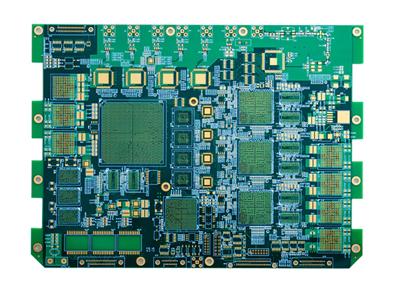
4-layer PCBs make routing easier, improve electrical stability, and better support modern circuit requirements.
2-layer boards can be sufficient for simple layouts, but dense routing, high-speed signals, and EMI constraints often push designs beyond 2 layers. For this reason, 4-layer PCBs are widely used in industrial, embedded, automotive, communications, and compact consumer electronics.
A 4-Layer PCB Stackup separates signals, power, and ground more effectively, improving routing efficiency, reducing noise, supporting better EMI performance, and enabling more practical impedance control. This guide covers the essentials: what a 4-layer PCB is, how it compares to a 2-layer board, how stackup choices affect performance, and the key design and manufacturing considerations.
What Is a 4-Layer PCB?
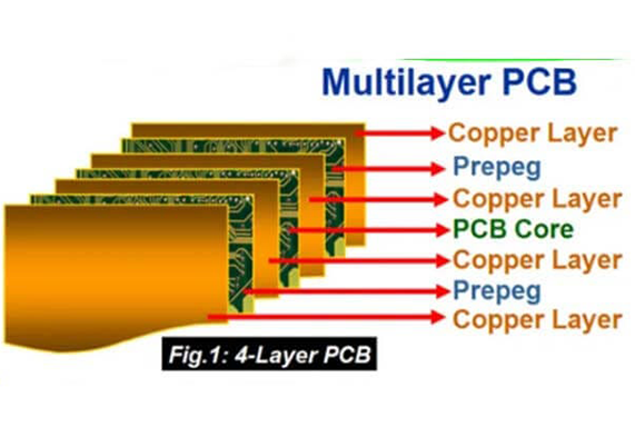
4-layer PCBs use four copper layers separated by insulating dielectric materials, forming one of the most common multilayer PCB constructions.
In most designs, the outer layers handle components and signal routing, while the inner layers serve as ground and power (or reference) planes.
Most 4-Layer PCB Stackup like this:
- Top layer — components and signal routing
- Inner layer 1 — ground plane
- Inner layer 2 — power plane
- Bottom layer — components and signal routing
Keeping signals close to a reference plane improves return paths, makes behavior more predictable, and simplifies EMI control.
In practice, four layers are more than “two extra copper layers.” The stackup enables cleaner routing, stronger grounding, and more consistent electrical performance.
2 Layer vs 4 Layer PCB: What Is the Real Difference?
2-layer boards work well for simple designs. 4-layer boards become the better choice when routing density, grounding quality, and signal behavior start to matter.
| Layers | Top and bottom only | Two outer layers plus two inner layers |
| Routing | Limited for dense layouts | More routing space and better organization |
| Grounding | Less continuous | Solid internal reference plane is possible |
| Signal integrity | Harder to control | Better return paths and more stable signals |
| EMI performance | Higher risk in complex designs | Better noise and EMI control |
| Best use | Simple, low-cost boards | Compact, higher-density, or mixed-signal boards |
For simple products, 2-layer designs are often enough. When layouts get tighter, grounding becomes critical, or performance margins shrink, 4-layer PCBs are usually the better choice.
Why Use a 4-Layer PCB?
4-layer PCBs are widely used because they balance performance and cost.
Compared with 2-layer boards, 4-layer designs provide a stronger electrical structure while remaining far more manageable than 6-layer or 8-layer builds for many applications.
Key benefits typically include:
- Better routing flexibility
- Cleaner power and ground organization
- Improved signal integrity
- Lower EMI risk
- Better support for moderate-speed digital interfaces
- More robust mixed-signal layout
Common product types using 4-layer boards include:
- Industrial control products
- Embedded systems
- Wireless communication modules
- Automotive electronics
- Measurement and sensing devices
- Compact consumer electronics
For many designs, four layers mark the point at which cost remains reasonable while the electrical structure improves significantly.
Common Applications of 4-Layer PCBs
4-layer PCBs are well-suited to a wide range of products where board area is limited and electrical performance matters.
1. Industrial Control Systems
PLC modules, sensor interfaces, motor-control logic, and automation electronics benefit from cleaner grounding and more predictable routing.
2. IoT and Embedded Devices
Smart modules, edge controllers, wireless nodes, and processor-based boards often require more routing capacity than two layers can provide.
3. Automotive Electronics
Control modules, monitoring systems, and interface boards often require greater stability and EMI performance in harsh environments.
4. Communication Equipment
Routers, gateways, and RF-related control boards benefit from improved signal reference and better layer organization.
5. Mixed-Signal Products
Designs combining analog sensing and digital processing require careful grounding and isolation between noisy and sensitive sections. Four layers make that separation easier to implement.
6. Compact Consumer Electronics
As features increase while mechanical space remains limited, four layers are often the most practical option.
4-Layer PCB Stackup Basics
Stackup refers to the layer order and dielectric spacing inside a 4-layer PCB. This is one of the most important design decisions because it directly affects:
- Signal integrity
- EMI / EMC performance
- Crosstalk
- Impedance control
- Manufacturability
Why Stackup Matters
Good stackups keep signals close to their reference planes, strengthen return paths, and make routing more predictable.
Poor stackups tend to increase noise, worsen crosstalk, and make controlled impedance harder to achieve. Stackup choices deserve early attention, not last-minute decisions.
Common 4-Layer PCB Stackup Formats
A common baseline stackup looks like this:
- Layer 1: Signal
- Layer 2: Ground
- Layer 3: Power
- Layer 4: Signal
This structure works well for many general-purpose digital boards and remains widely supported by manufacturers.
Another common option:
- Layer 1: Signal (or mixed signal/power)
- Layer 2: Ground
- Layer 3: Ground (or power)
- Layer 4: Signal (or mixed signal/power)
This approach can be more effective when both outer layers carry important routing and need strong reference planes.
How to Choose the Right Stackup
Stackup selection should follow electrical goals, not habit.
- General digital boards: Signal–Ground–Power–Signal is often sufficient.
- Higher-speed layouts: Strong referencing for both outer signal layers becomes more important.
- Mixed-signal designs: Separation and clean return paths matter as much as routing space.
- Power + control boards: Power distribution must improve without sacrificing signal reference quality.
4-Layer Impedance Stackup: What Designers Need to Know
Controlled impedance on a 4-layer PCB depends on the stackup, not just trace width.
Key contributors include:
- Dielectric thickness
- Material dielectric constant (Dk)
- Copper thickness
- Trace geometry
- Distance to a solid reference plane
- Fabricator’s available stackup constructions
As a result, a 50-ohm trace on one 4-layer board may require a different width on another, even with the same layer count. Dielectric spacing and materials vary.
Best practice is simple: confirm the intended stackup with the PCB manufacturer before finalizing impedance-critical routing. This prevents a common failure mode—designing trace widths for an assumed construction while fabrication uses a different standard build.
4-Layer PCB Design Guidelines
Four layers provide more freedom, but strong results still depend on disciplined layout practices.
1. Keep signal layers adjacent to solid reference planes
Continuous reference planes improve return paths and reduce noise.
2. Avoid routing across split planes
Crossing a plane gap breaks the return current flow and can cause EMI and signal-quality problems.
3. Keep return paths short and continuous
Fast edges, clocks, and sensitive analog nodes depend on controlled return currents.
4. Route critical nets first
Clocks, differential pairs, and sensitive analog paths should be placed before less critical routing consumes space.
5. Control spacing to reduce crosstalk
Aggressive nets routed too closely will couple. Maintain spacing based on speed and sensitivity.
6. Use vias intentionally
Unnecessary layer transitions complicate routing and can degrade performance on critical nets.
7. Plan power early
Power distribution and decoupling paths should be planned from the start, not treated as leftover routing.
4-Layer PCB Manufacturing Basics
4-layer PCBs are built by laminating copper foils, prepreg, and core materials into a single multilayer structure.
The process typically follows this sequence:
- Inner layers are patterned and etched.
- The stack is laminated under heat and pressure.
- Holes are drilled and plated.
- Outer layers are patterned and etched.
- Solder mask and surface finish are applied.
- Electrical testing and inspection are completed.
From a production standpoint, 4-layer boards are standard, but stackup choices still affect yield, impedance consistency, and cost. Board thickness, copper weight, dielectric spacing, and impedance targets should align with realistic fabrication capability.
Common finished thicknesses include:
- 0.8 mm
- 1.0 mm
- 1.2 mm
- 1.6 mm
- 2.0 mm
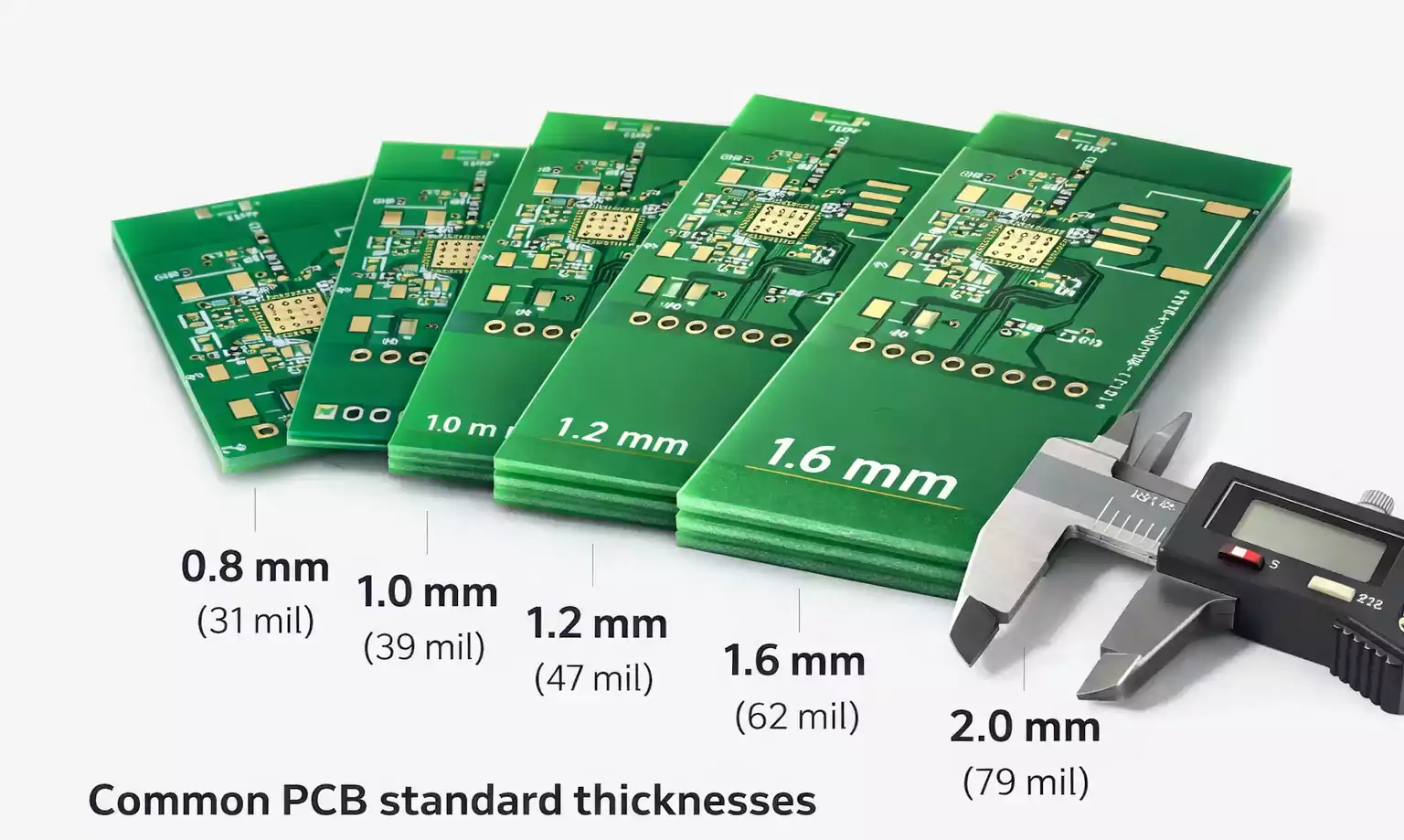
Among these, 1.6 mm remains one of the most common standards for general electronics. Thinner or thicker options may be chosen based on mechanical requirements, connector constraints, or electrical targets.
Key Things to Confirm Before Manufacturing
Before releasing a 4-layer PCB to fabrication, confirm the items below.
| Finished board thickness | Affects mechanical fit, dielectric spacing, and impedance behavior |
| Copper weight | Impacts current capacity and trace geometry |
| Impedance requirements | Determines whether standard or custom stackup is needed |
| Material system | Affects thermal, electrical, and reliability performance |
| Standard vs custom stackup | Influences cost, manufacturability, and signal performance |
FAQ
What is a 4-layer PCB?
A 4-layer PCB is a multilayer circuit board with four copper layers separated by insulating dielectric materials. Outer layers typically carry signals and components, while inner layers provide ground and power planes.
What is the difference between 2-layer and 4-layer PCBs?
2-layer boards use only the top and bottom copper layers. 4-layer boards add two internal layers, improving routing capacity, grounding, power distribution, and signal behavior.
What is the best 4-Layer PCB Stackup?
No single stackup fits every design. Signal–Ground–Power–Signal is a common starting point, while two-reference-plane approaches can perform better for higher-speed or noise-sensitive layouts.
What is a typical 4-layer PCB thickness?
1.6 mm is common, with 0.8 mm, 1.0 mm, 1.2 mm, and 2.0 mm also widely used depending on mechanical and electrical needs.
Do 3-layer PCBs exist?
3-layer boards exist but are uncommon. Even layer counts are typically preferred for balanced construction and standard manufacturing workflows.
Conclusion
4-layer designs are often the most practical upgrade from a basic 2-layer board. Better routing flexibility, cleaner grounding, improved EMI performance, and more controlled electrical behavior are achievable without incurring the added cost and complexity of 6-layer or 8-layer structures.
Performance depends on more than layer count. Effective stackup planning, solid reference planes, realistic impedance control, and alignment with manufacturing constraints drive stable results.
When these factors are properly managed, a 4-layer PCB Stackup delivers a strong balance of performance, reliability, and cost. For multilayer PCB projects, working with an experienced manufacturer such as FastTurnPCB helps ensure consistent production quality and smoother execution.
