After system definition, functional partitioning, simulation, and placement are complete, the high-speed PCB design work enters its most critical phase.
At this point, the goal is no longer proving the schematic works. The goal is to ensure the physical design can withstand real edge rates, routing density, fabrication limits, and production repeatability. In other words, this is where the PCB design flow transitions from design intent to manufacturable reality.
This guide covers the second half of the PCB design flow for high-speed PCB design, with a focus on high-speed PCB routing, PCB signal integrity, PCB timing analysis, PCB routing constraints, PCB routability analysis, and the release of complete PCB manufacturing files.

PCB Routing Constraints: Signal Integrity Starts Before High-Speed PCB Routing
In low-speed designs, logical connectivity is often enough. In high-speed PCB design, it isn’t.
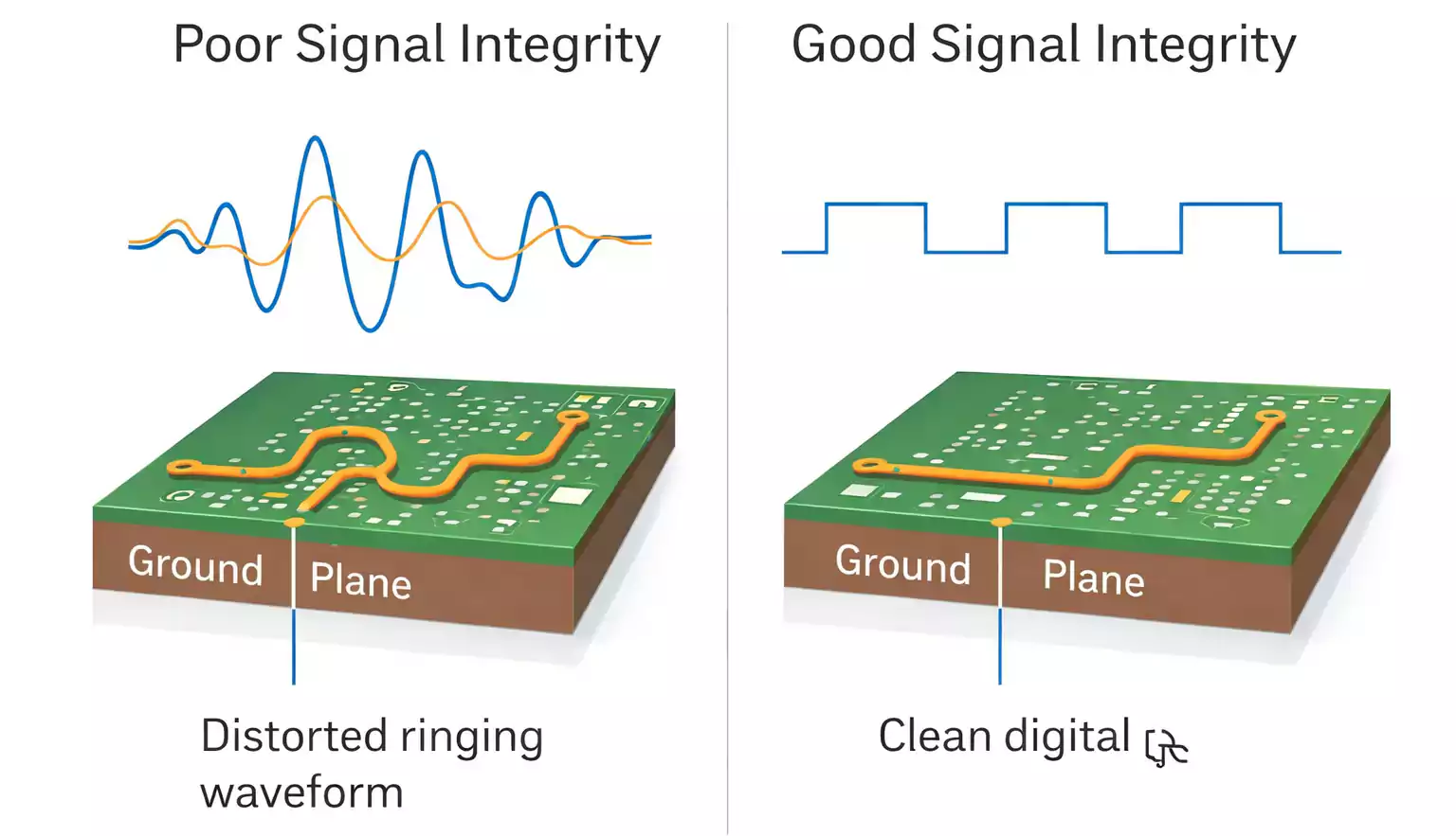
As edge rates increase and interconnect delays become significant, traces behave like transmission lines. That’s when layout geometry directly impacts PCB signal integrity. Common failure modes include:
- Reflections
- Crosstalk
- Ringing
- Overshoot and undershoot
- False switching / threshold errors
Therefore, define and review routing constraints immediately after placement—before detailed high-speed routing.
Key constraints typically include:
- Driver-to-load topology
- Termination strategy and placement
- Node ordering along the net
- Trace length control and skew limits
- Impedance consistency (single-ended and differential)
The objective is predictable transmission behavior before copper is committed. In high-speed backplanes and compute platforms, these constraints are essential—small physical choices can lead to significant instability.
PCB Timing Analysis and Transmission Line Modeling: Predict Before You Route
Once placement is stable, physical positions and approximate routing corridors are known. Even before detailed routing, this enables early PCB timing analysis and transmission line modeling based on:
- Estimated trace lengths and flight times
- Topology assumptions (point-to-point vs. multi-drop)
- Early risk signals for reflection and edge distortion
Because node coordinates and connection order are defined, designers can simulate likely behavior and identify timing margin problems while changes are still easy.
The value here is straightforward: fixing PCB signal integrity issues after routing is expensive; identifying them before high-speed PCB routing is efficient and controlled. For mature high-speed PCB design teams, early timing and interconnect modeling is a standard risk-reduction step in the PCB design flow.
PCB Signal Integrity Noise: Internal Noise vs. External Interference
Not all noise has the same cause, and treating every noise problem the same leads to ineffective mitigation. A cleaner PCB signal integrity approach is to separate noise into two categories.
1. Internal System Noise (Intrinsic)
This includes:
- Thermal noise
- Switching noise
- Intrinsic signal noise
Internal noise is part of normal circuit behavior. It can’t be eliminated, but it can be managed by improving the signal-to-noise ratio and controlling the physical implementation, including return paths, decoupling, and edge-rate management.
2. External Interference (Coupled / Environmental)
External noise originates outside the immediate circuit and can be especially damaging in sensitive analog, RF-adjacent, and mixed-signal areas.
Typical mitigations include:
- Shielding
- Grounding strategy improvements
- Physical isolation of sensitive blocks
- Filter networks
- Controlled interface design
Understanding whether the issue is intrinsic or external helps choose the right fix and speeds debugging.
If Timing or SI Fails, Revisit Placement and Topology (Before Routing)
If early modeling reveals:
- Excessive delay
- Poor timing margin
- Significant reflections
- Edge distortion or ringing
The correct response is not to “route it and see.” In high-speed PCB design, this is where you revise placement and topology.
Common corrective actions include:
- Moving critical components closer together
- Shortening priority signal paths
- Revising topology (point-to-point vs. multi-drop)
- Adding, removing, or relocating termination
- Adjusting stackup strategy to support constraints
In GHz-class digital systems—especially on physically large boards—layout length and topology directly impact global timing behavior. Iteration at this stage increases first-pass success and prevents late-stage reroutes.
PCB Routability Analysis: Confirm You Can Route the Board You Placed
Many designs fail not from electrical errors but from underestimated routing resources. Routability analysis should occur before detailed routing.
Routability checks should answer:
- Do you have enough signal layers?
- Is placement spacing realistic for the expected fanout?
- Where are the congestion hot spots?
- Are critical channels blocked by mechanical or keepout constraints?
- Does the floorplan support the intended stackup and via strategy?
Most modern EDA tools provide congestion metrics and routing feasibility checks. If routability is weak, the right fix is usually a revision of the placement/layer strategy—not forcing compromised routing.
This step is especially important in high-density multilayer boards and mixed-signal layouts where PCB routing constraints reduce usable routing real estate.
High-Speed PCB Routing: Execute Within Constraints, Not Against Them
Once placement, PCB timing analysis, and PCB routability analysis are in good shape, detailed high-speed PCB routing begins.
Routing must comply with the constraints defined earlier, including:
- Trace width and spacing rules
- Length matching and skew control
- Impedance requirements
- Differential pair coupling and symmetry
- Return path continuity
- Crosstalk limits and spacing classes
In practice, high-performing teams typically use:
- Manual routing for critical high-speed nets
- Controlled routing for power distribution paths
- Automated routing for non-critical signals
- Post-route cleanup and optimization
A routing “playbook”—layer policy, via rules, net class priorities, and review criteria—improves consistency and reduces review churn in multi-engineer designs.
Post-Route Verification: Close the Loop on SI, Timing, and Connectivity
Finishing routing doesn’t mean the design is done; now, actual lengths and geometries require re-validation.
Post-route checks typically include:
1. Re-check PCB Signal Integrity and PCB Timing Analysis
- Confirm timing margins using actual trace lengths.
- Re-check reflection behavior and edge quality
- Evaluate coupling risks for adjacent aggressor/victim nets.
2. Netlist / Connectivity Verification
- Ensure no unintended connectivity changes occurred.
- Verify no opens/shorts were introduced during edits.
3. Manufacturability and Rule Compliance
- Confirm trace width/spacing compliance.
- Validate solder mask clearances.
- Ensure pads are not accidentally exposed or covered.
- Confirm impedance structures are manufacturable.
These checks are where many “it worked in CAD” problems are prevented from becoming “it failed at build.”
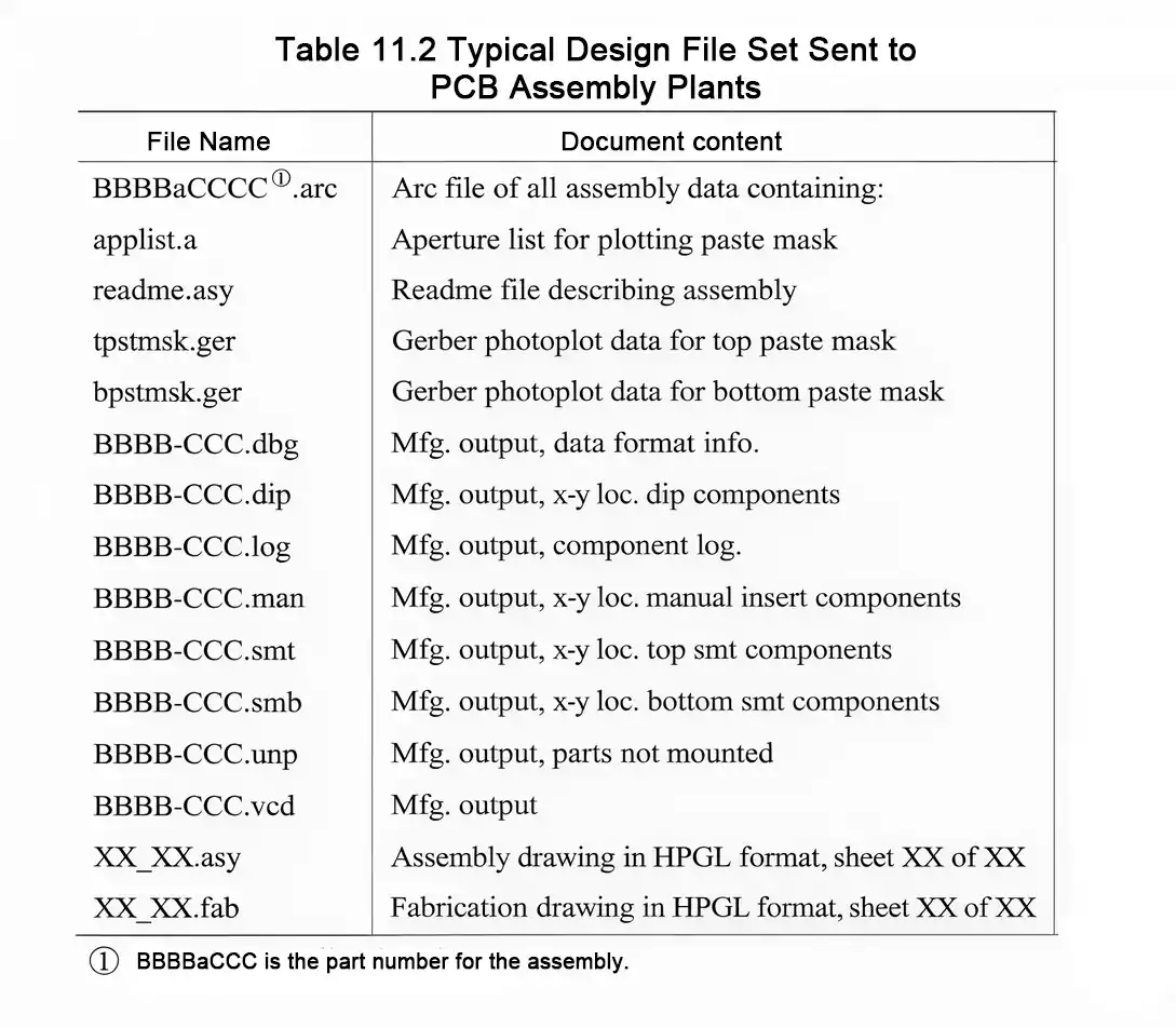
PCB Manufacturing Files: From Design Database to Production-Ready Release
Once verification is complete, the PCB design flow transitions into manufacturing release. A complete release package typically includes:
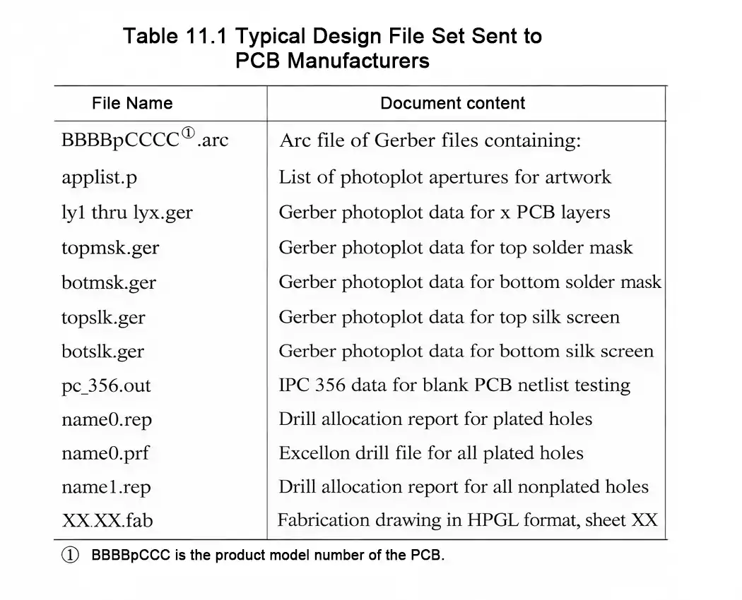
- Fabrication outputs (Gerber or ODB++)
- Drill files
- Pick-and-place data
- Assembly drawings
- Bare-board test data (as applicable)
- Functional test documentation (as applicable)
- Complete, validated BOM
These PCB manufacturing files are what fabricators and assemblers actually use. Any ambiguity here leads to delays, scrap risk, and yield loss. For B2B hardware, the clarity and completeness of manufacturing files are directly tied to lead time, repeatability, and scalability.
Design Archiving: Protecting the High-Speed PCB Design Asset
Final step: structured archiving.
Archiving isn’t just backup. It supports:
- Future revisions and ECOs
- Field failure investigation
- Version traceability
- Long-term lifecycle management
A complete archive should include the native database, manufacturing outputs, test documents, revision history, and engineering notes. Inability to reproduce a design later becomes a business risk, not just an inconvenience.
Final Thoughts: High-Speed PCB Design Depends on a Disciplined PCB Design Flow
The second half of the PCB design flow determines whether a high-speed PCB design reaches production smoothly or enters an expensive debug loop.
When PCB routing constraints, PCB timing analysis, PCB routability analysis, and disciplined high-speed PCB routing are executed as a connected process—and verified with real physical data—the result is a board that:
- Manufactures consistently
- Assembles reliably
- Passes test efficiently
- Scales to volume
- Supports long-term maintenance
That’s the difference between a board that works in the lab and a product that ships reliably.