

Even after a perfect layout, flawless fabrication, and a seemingly smooth SMT run, one common problem can turn an otherwise great build into a costly rework cycle: board warpage.
That slight bow or twist—sometimes barely noticeable—can disrupt component alignment, degrade solder joint quality, and create hidden reliability risks that show up months later in the field.
This guide explains what board warpage is, why it matters for assembly and signal performance, and the practical steps designers, fabricators, and assembly teams can take to avoid it.
What Is Board Warpage (PCB Warpage)?
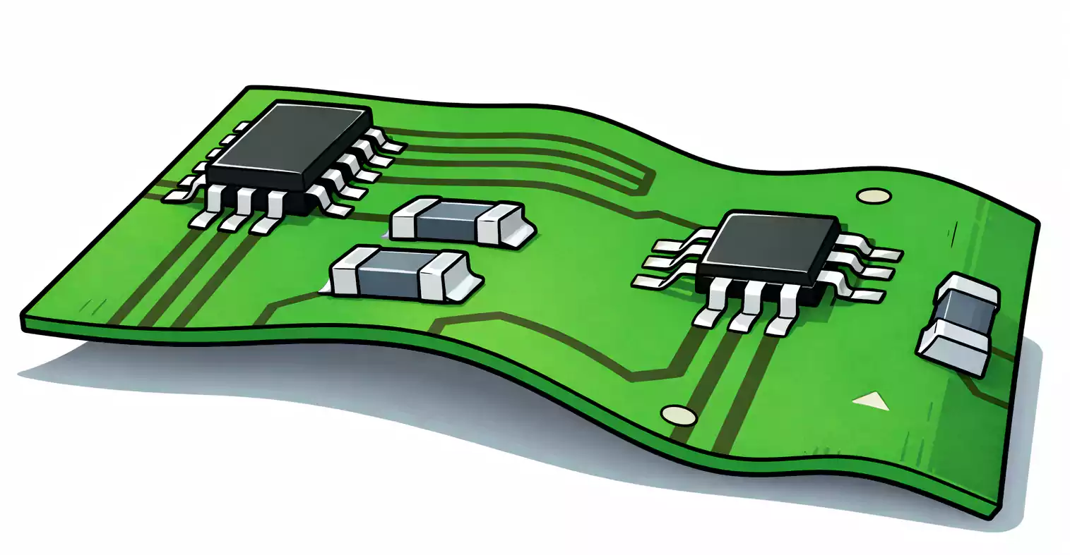
Board warpage is the bending or twisting of a printed circuit board so that it no longer lies flat. Instead of remaining planar, the PCB becomes deformed due to mechanical or thermal stresses during fabrication, storage, or reflow soldering.
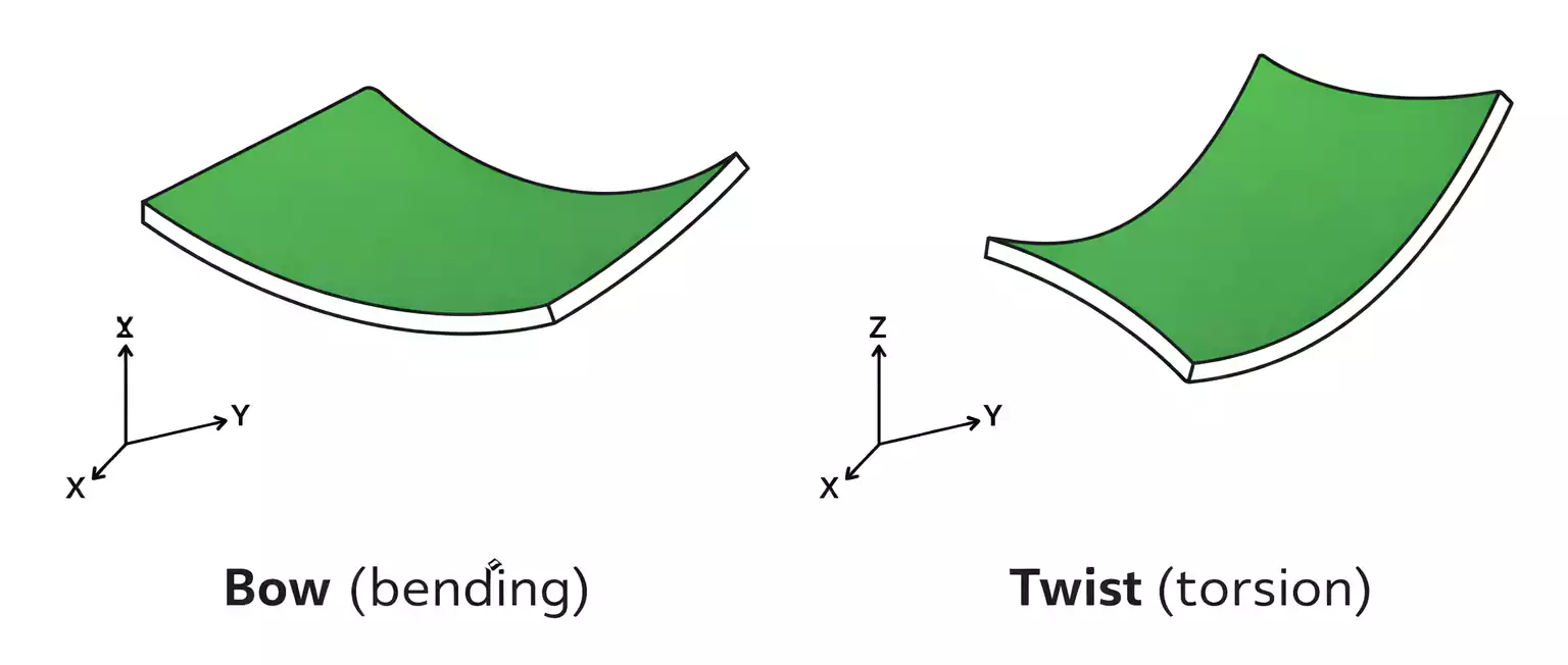
There are two primary shapes of PCB deformation:
1. Bow
The entire board curves like an arc across its length or width. All corners typically remain in the same plane, but the center rises or sinks.
2. Twist
One corner lifts above the plane while the others remain flat, creating a twisted, propeller-like shape.
This is more problematic for component alignment because the angle creates non-uniform coplanarity across the PCB.
Both bow and twist are types of warpage, often sharing causes, but distinguishing them aids diagnosis and prevention.
Why Does Warpage Affect Component Alignment and Even Signal Integrity?
Many engineers view warpage solely as an SMT solderability issue, but its effects extend far beyond manufacturing yield.
1. Impact on Component Alignment (Most Visible, Most Expensive)
A warped PCB no longer presents a flat mounting surface. That directly affects:
- Coplanarity of pads for BGAs, QFNs, QFPs, and connectors
- Placement accuracy during pick-and-place
- Solder paste contact between the stencil and the pads.
- Reflow wetting behavior, increasing risks of:
- Opens
- Head-in-pillow
- Voids
- Bridges
- Tombstoning
A board that bends by just a fraction of a millimeter can produce thousands of dollars of scrap or rework.
2. Indirect Impact on Signal Integrity
Warpage does not directly change impedance—but it does influence the mechanical conditions under which high-speed components and connectors operate.
For example:
- Misalignment in high-speed connectors → intermittent contact
- Stress on cage-mounted or press-fit components → micro-fractures and SI jitter
- Forced mechanical fit when assembling warped boards → stress on reference planes or solder joints
In short, Poor flatness compromises the electrical environment, especially in high-speed, high-density designs.
How Much PCB Warpage Is Acceptable?
Industry practice follows commonly accepted limits for bow and twist:
- ≤ 0.75% of board diagonal length for SMT assemblies
- ≤ 1.5% for non-SMT applications
Example:
If a PCB’s diagonal is 300 mm, the allowed warpage is:
0.75% × 300 mm = 2.25 mm
Anything beyond this threshold typically results in placement errors, coplanarity failures, or functional misalignment of connectors.
Why Do PCBs Warp?
Board warpage is due to stress imbalance: copper, glass fiber, and resin expand or contract at different rates when heated or cooled, creating asymmetrical movement that bends the board toward the faster-shrinking side.
1. Asymmetrical Stackup
If dielectric thickness, copper weights, or resin content are not mirrored top-to-bottom, stresses accumulate unevenly during lamination and reflow.
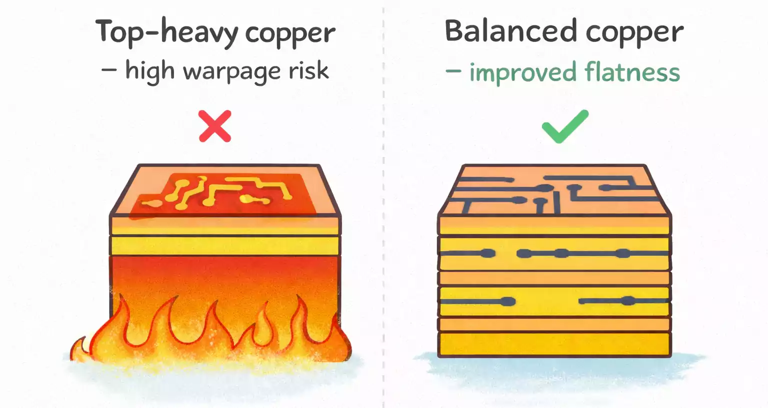
2. Uneven Copper Distribution
Large copper areas heat and cool differently from sparse regions.
This leads to localized shrinkage or expansion, bending the PCB.
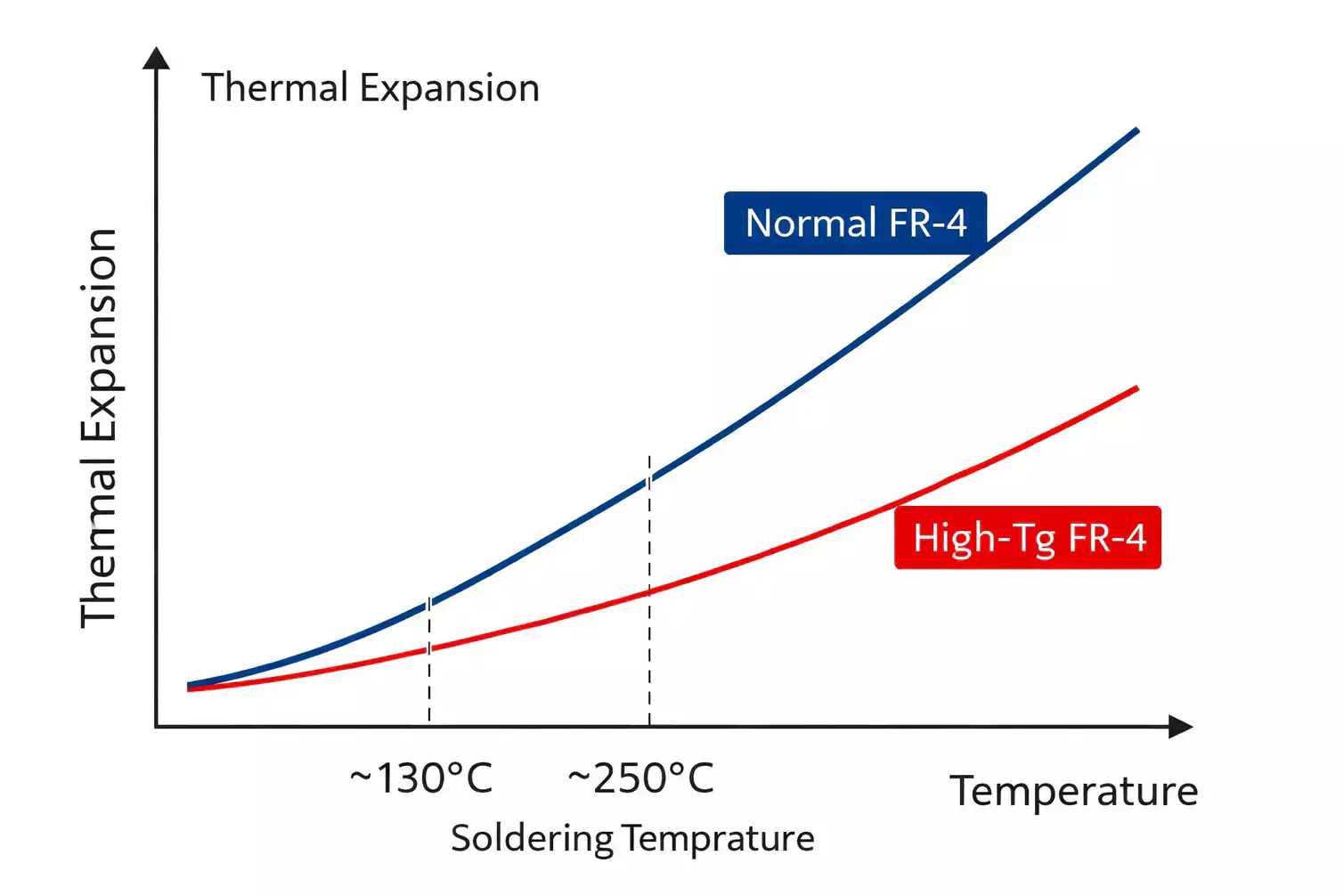
3. Material Limitations—Low Tg, High CTE
Materials with a low glass transition temperature (Tg) soften significantly during reflow.
- Soft materials = more deformation under gravity
- High CTE laminates = greater expansion and contraction
Thin boards (0.8 mm or below) are particularly vulnerable.
4. Moisture Absorption
FR-4 is hygroscopic. Moisture trapped in the laminate can vaporize during reflow, leading to internal pressure, microdelamination, and warpage.
5. Lamination and Process-Induced Residual Stress
During PCB fabrication:
- Over-pressure
- Uneven resin flow
- Inconsistent cooling rates
- Poor press cycle control
…can embed internal stress that emerges later during reflow.
6. Reflow Thermal Profile and Support During Heating
Fast heating or cooling traps uneven thermal gradients.
Also, a PCB softens above Tg; without proper support, the board sags under its own weight or component mass.
In short:
Warpage begins during fabrication but is often visible only during assembly.
Practical Ways to Prevent Board Warpage (PCB Warpage)
Below are the techniques with the highest real-world impact—prioritized from design to assembly.
1. Design a Symmetrical, Balanced Stackup
The most effective prevention technique is simply keeping the PCB structure balanced.
- Mirror dielectric layers across the center plane
- Keep copper weights symmetrical.
- Avoid one-sided heavy copper or large ground pours.
- Maintain even material distribution around cavities or cutouts.
Balanced stackup = balanced thermal expansion = minimal warpage.
2. Maintain Uniform Copper Distribution
Copper imbalance is one of the top contributors to PCB warpage.
Guidelines:
- Avoid placing large copper planes on only one side.
- Consider cross-hatching or copper-thieving in sparse regions.
- Maintain similar copper density across all layers.
- Add copper to breakaway rails so that panel edges heat and cool consistently.
Uneven copper density creates uneven stiffness and thermal behavior—leading to predictable bending.
3. Choose High-Tg Materials for Demanding Applications
High-Tg laminates offer:
- Better dimensional stability
- Lower CTE above Tg
- Less softening during lead-free reflow
Use high-Tg materials when the design includes:
- Dense BGAs
- Heavy components
- Large or thin boards
- Double-sided assembly
- Extended reflow cycles
This single change dramatically reduces the risk of warpage.
4. Control Moisture: Proper Storage and Pre-Bake
Since FR-4 absorbs moisture, boards should be stored:
- In sealed packaging
- With desiccant and humidity indicators
- Under controlled humidity conditions (typically < 30% RH)
If boards have been exposed to air:
- Pre-bake according to laminate specifications (commonly 110–125°C for several hours)
Pre-baking removes moisture that could otherwise cause expansion or delamination during reflow.
5. Strengthen Panels Using Rigid Rails
Add mechanical strength to the PCB panel by including:
- Break-off rails
- Sidebars
- Crossbars (if panel size allows)
These rails prevent deformation as the panel softens during reflow.
They are removed after assembly, but they perform an essential function during the thermal cycle.
6. Optimize the Reflow Profile
A reflow soldering profile that heats too fast or cools too aggressively increases thermal stress.
Best practices:
- Use a gentle preheat ramp (about 1–2°C per second)
- Ensure even heating across the PCB.
- Allow controlled cooling after peak temperature.
The goal is to minimize temperature gradients between layers, reducing stress mismatch.
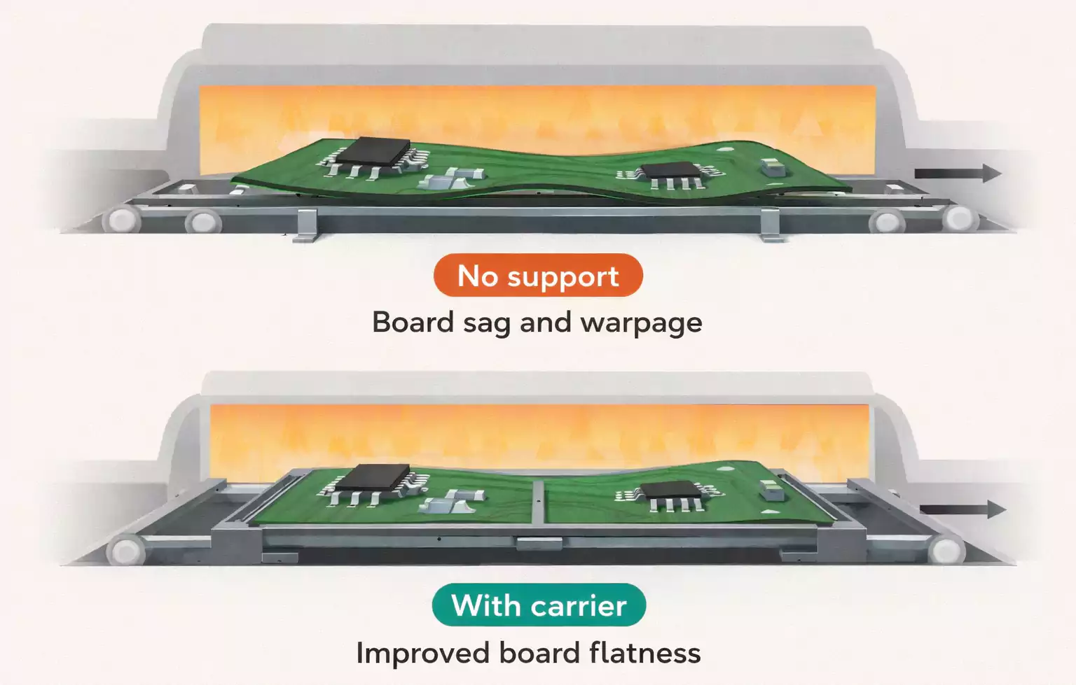
7. Use Supports, Pallets, or Carriers During Reflow
Once a PCB exceeds Tg, it becomes flexible. Without support, it may sag.
Use:
- Stainless steel or composite carriers
- Center support rails
- Dedicated reflow fixtures
- Edge support if the panel width is large
This technique is essential for:
- Thin boards
- Heavy assemblies
- Long panels
- Flexible-rigid products
Pallets and carriers keep boards flat during their most vulnerable state.
8. Improve Fabrication Process Control
Board warpage often begins at the fabrication stage.
Key controls include:
- Stable lamination press cycles
- Controlled cooling and de-stacking
- Resin flow management
- Quality incoming material with consistent Tg and CTE
- Flatness inspection after lamination and routing
While designers cannot directly modify the PCB factory’s process, choosing suppliers with strong process control is one of the most powerful ways to prevent warpage.
9. Post-Assembly Flattening (Last Resort)
Some assembly houses use heated plates or mechanical presses to flatten mildly warped boards.
This is not ideal because:
- It cannot fully eliminate internal stress.
- Repeated heating cycles degrade laminate properties.
- It’s not a reliable mass-production solution.
Use only for urgent recovery—not as a standard practice.
Quick Ways to Check for PCB Warpage
Even without specialized equipment, engineers can identify warpage early.
1. Flat-Surface “Rocking” Test
Place the PCB on a granite block or flat glass surface.
Press one corner:
- If the opposite corner lifts → twist
- If the center lifts → bow
Simple, fast, and catches 90% of problematic cases.
2. Basic Quantitative Method
Measure:
- Board diagonal length
- Maximum out-of-plane height at the worst point
Use the formula:
Warpage % = (Max Height ÷ Diagonal Length) × 100%
Compare with the 0.75% limit commonly used for SMT applications.
3. Inspect Before and After Reflow
Checking flatness before and after reflow helps determine:
- Whether warpage is intrinsic (from fabrication)
- Or extrinsic (from assembly conditions)
This greatly speeds up troubleshooting.
Troubleshooting Checklist: When Warpage Appears, Check These First
1. If warpage only appears after reflow:
- Reflow profile too aggressive
- Insufficient board support
- Large panel size with weak rails
- Moisture not removed before assembly.
2. If the board is already warped on arrival:
- Asymmetrical stackup
- Copper imbalance
- Improper lamination/cooling
- Material inconsistencies
- Poor packaging or storage conditions
3. If only certain positions on the panel warp:
- Panel design imbalance
- Rails with insufficient copper
- V-cut weakening the panel.
- Incorrect depaneling or stacking method
Conclusion
Board warpage is one of the most common—and most preventable—reliability and assembly issues in PCB manufacturing.
By focusing on a balanced stackup, even copper distribution, proper materials, and controlled thermal/mechanical handling during assembly, engineers can eliminate most warpage problems before they ever reach the SMT line.
Reliable flatness means better component alignment, more stable signal performance, and far fewer production delays.
If you need consistent PCB flatness and manufacturing stability, FastTurnPCB provides high-quality fabrication and assembly processes designed to minimize warpage from the ground up.