

CAF failures rarely show up during prototyping. Boards pass electrical tests, early functional checks, and often perform flawlessly in the lab. Then—after months or years in the field—something subtle appears: unexpected resets, leakage on previously quiet nets, intermittent high-speed signal loss, or a catastrophic short.
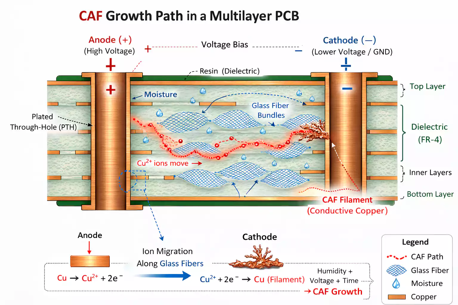
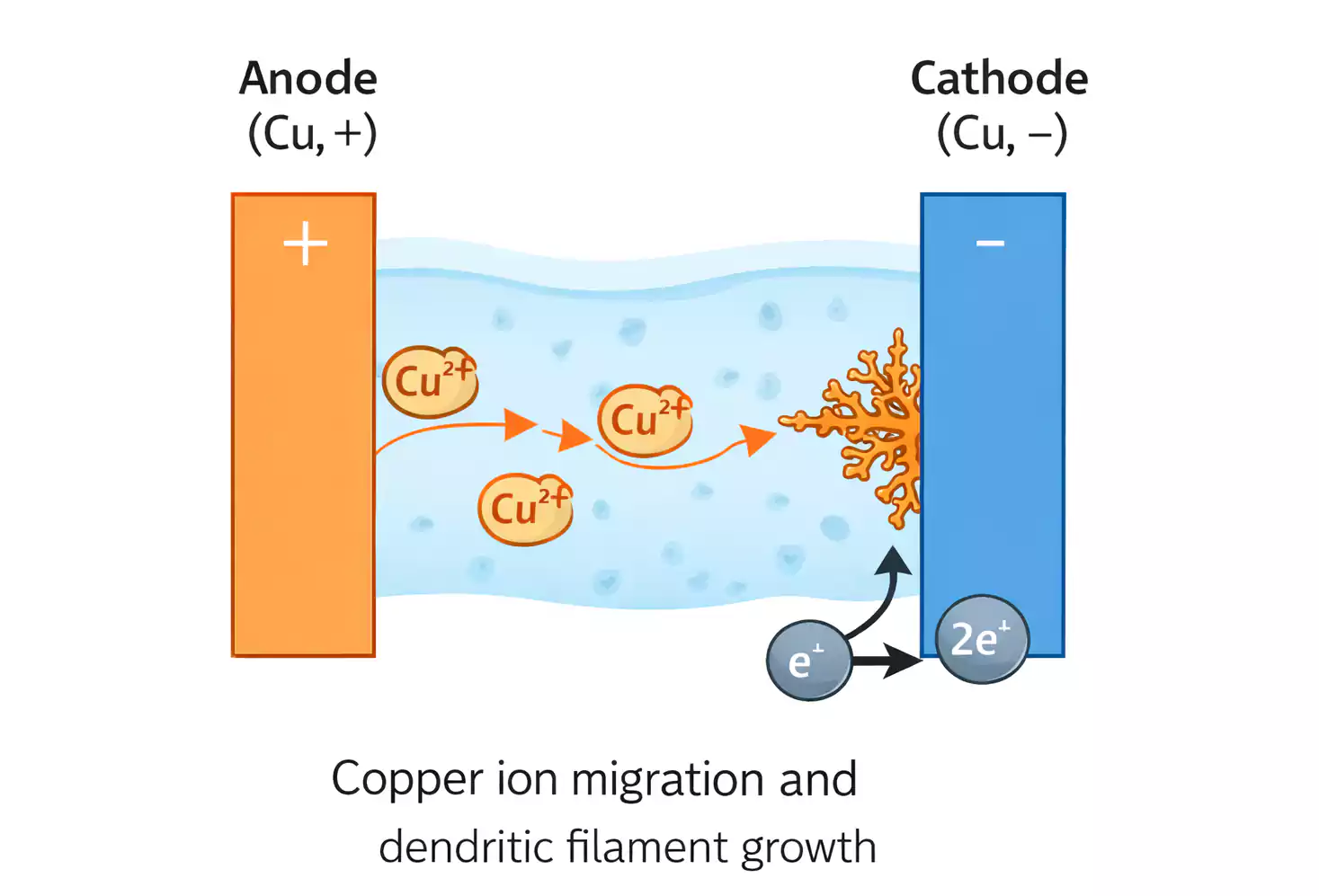
The culprit in many extended reliability investigations is Conductive Anodic Filament (CAF): a hidden, internal copper filament that slowly grows through the PCB dielectric until it forms a conductive bridge between two conductors that were never meant to touch.
This article explains what CAF is, why it forms, and—most importantly—how to design PCBs that actively prevent CAF growth.
What Exactly Is CAF, and Why Does It Cause Field Failures?
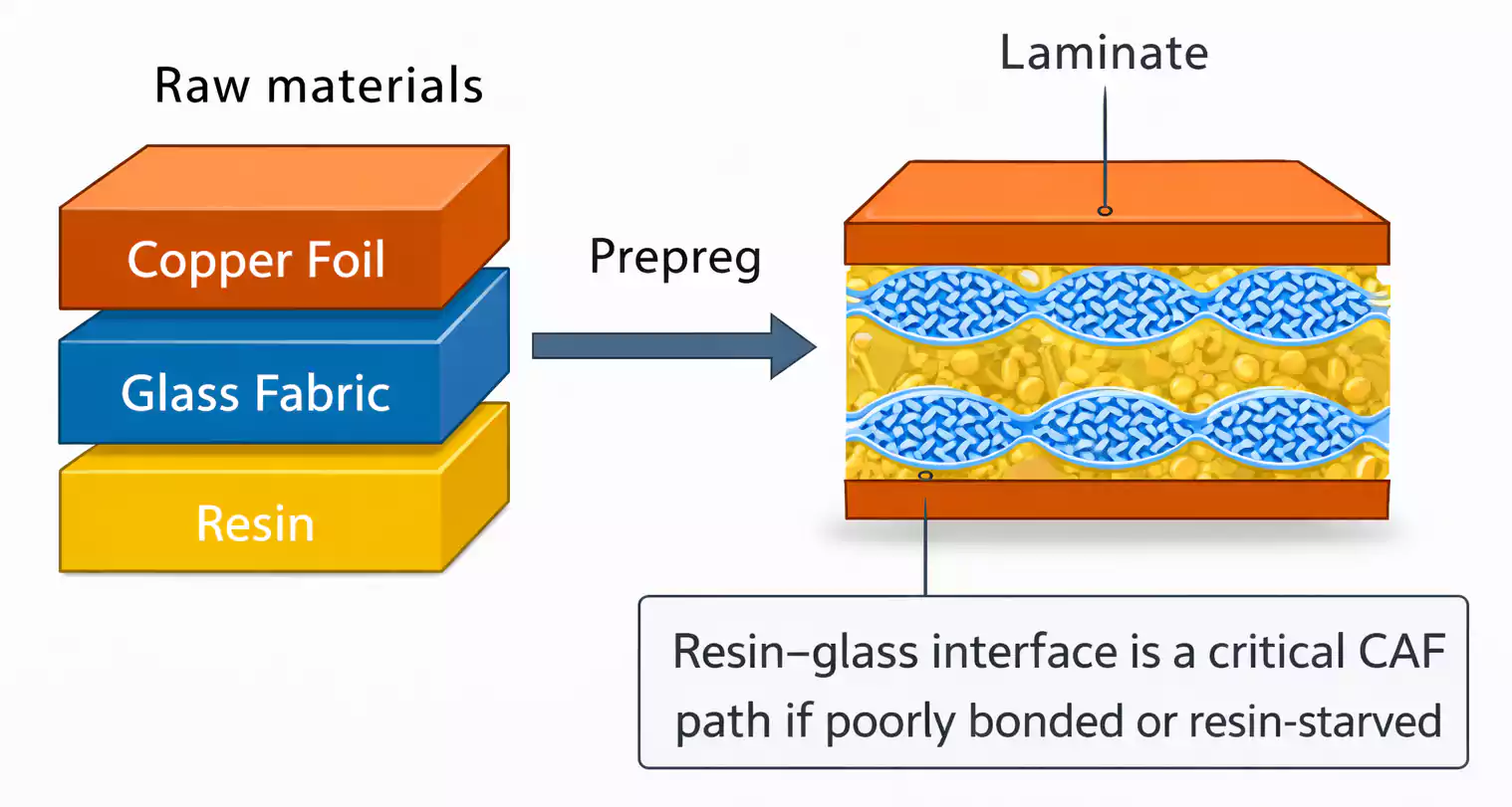
Conductive Anodic Filament (CAF) is an internal electrochemical failure mode in printed circuit boards. Instead of forming on the surface, CAF grows inside the laminate, typically along the interface between glass fiber bundles and the resin system. As moisture enters the board and a voltage differential is present, copper ions migrate from an anode toward a cathode, depositing metallic growth that eventually forms a conductive path.
CAF is dangerous because:
- It is invisible—you can’t see it during visual inspection.
- It progresses slowly, meaning boards appear good early and then fail later.
- It produces intermittent, hard-to-reproduce field issues.
- It can result in microamp leakage, logic upset, or full short circuits.
In short, Conductive Anodic Filament is a latent reliability risk—one that only appears when the right stress conditions combine: humidity, voltage, time, and the right (or wrong) material structure.
Why CAF Happens: The Three Conditions Required for Filament Growth
The mechanism behind CAF is fundamentally electrochemical, not purely electrical. Three conditions must exist simultaneously:
- Moisture inside the PCB
Humidity absorbed into the dielectric (especially FR-4) reduces insulation resistance and provides an ionic pathway. - A voltage bias between two conductors
Higher DC voltage accelerates the dissolution and migration of copper ions. - A susceptible material pathway
The resin–glass interface, voids, microcracks, and resin-poor areas create physical channels where copper ions can migrate.
The Electrochemical Sequence of CAF Growth
- Moisture enters the board.
- A voltage differential causes copper to dissolve at the anode.
- Copper ions migrate along the glass/resin interface.
- They reach the cathode and plate out as a metal filament.
- Leakage increases, then a hard short forms.
CAF thrives within environments with high humidity, sustained DC bias, and long operational lifetimes—exactly the profile of automotive, telecom, industrial, aerospace, and medical electronics.
When Should a Project Team Care About CAF?
Conductive Anodic Filament is most critical in projects that involve:
- High humidity or condensation exposure
- Long product lifetimes (5–15 years or more)
- Sustained DC voltage differences between nets
- Dense via fields and multilayer stackups
- Thin dielectrics or HDI construction
- Automotive, aerospace, telecom, or industrial reliability requirements
If your design will be exposed to moisture,voltage, and time, then CAF must be treated as a design constraint, not an afterthought.
PCB Layout Rules to Prevent CAF Growth
A Practical, Engineering-Focused Guide
Most CAF mitigation happens not in materials, manufacturing, or testing—but at the design desk. Good layout practice dramatically reduces CAF susceptibility before the PCB ever reaches fabrication.
Here are the six most effective layout rules.
1. Increase Spacing Between Conductors at Different Potentials
Voltage difference is one of the primary accelerators of CAF. Increasing separation lengthens the migration path and reduces the field strength between conductors.
Key areas to increase spacing:
- Via-to-via spacing, especially inner layers
- Trace-to-via spacing
- Opposite-polarity nets in plane splits or cutouts
- High-voltage nets in dense routing regions
Inner layers deserve extra spacing margin because moisture tends to accumulate near the glass weave where CAF pathways form.
2. Remove Unconnected Pads and Inner-Layer Copper Islands
Orphan pads and unused copper shapes on internal layers create:
- Resin-poor regions
- Moisture traps
- Stress concentrators
All of which makes Conductive Anodic Filament more likely.
If a pad is needed solely for drill support, follow your fabricator’s guidance to retain only the minimal copper annulus instead of a large unused copper island.
3. Stagger Vias at ~45° to Avoid Straight-Line Copper-to-Copper Paths
Straight-line alignment of opposite-polarity vias creates a direct geometric pathway for ion migration.
A simple fix:
- Rotate via pairs by roughly 45 degrees.
- Or offset alternating vias by 1–2 pitches.
Breaking the straight path significantly reduces the probability of CAF because copper ions must travel a longer, increasingly tortuous route through the glass fibers.
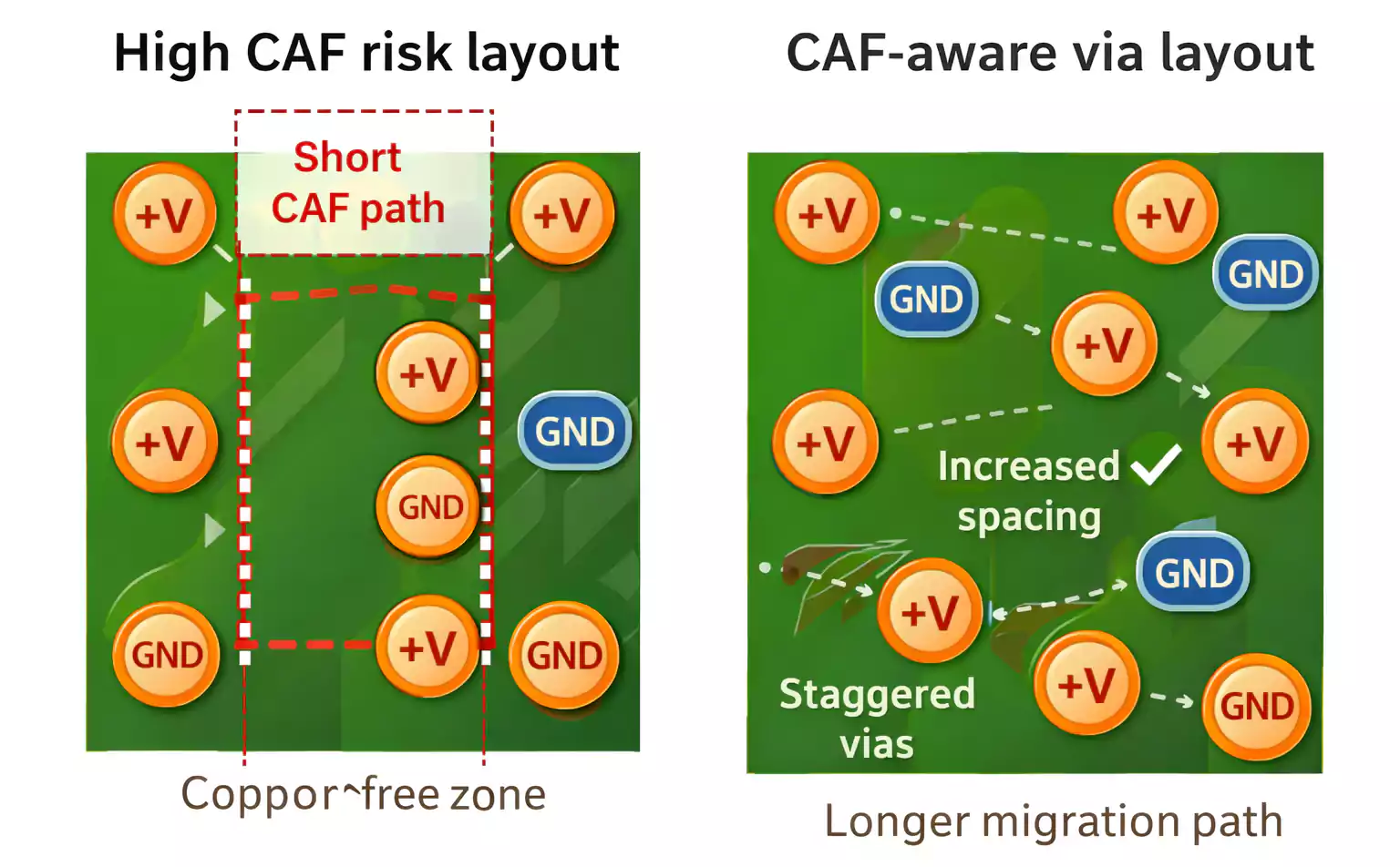
4. Plan Via Spacing and Avoid Long Parallel Rows of Opposite-Polarity Vias
Conductive Anodic Filament loves long, parallel, closely spaced vertical structures such as via barrels. When those vias carry different potentials, the risk multiplies.
Best practices:
- Avoid via rows that run parallel for long distances.
- Increase drill-to-copper spacing beyond the fabricator's absolute minimum.
- For high-reliability boards, add 0.1–0.2 mm extra clearance as a design rule.
- Offset via columns to disrupt continuous CAF pathways.
Treat drill-to-copper rules as reliability requirements, not just manufacturability constraints.
5. Avoid Dense Via Farms Wherever Possible
Large via clusters—especially under BGAs—can create:
- Micro-crack zones
- Local resin depletion
- Capillary channels for moisture ingress
- High electric field regions
If dense vias are unavoidable:
- Fan out in multiple stages instead of a tight burst.
- Insert local copper voids (keepouts) between nets with different potentials.
- Avoid clustering analog, digital, and power-return vias.
Small structural changes can drastically reduce CAF risk.
6. Use Teardrops at Pad-to-Trace and Via-to-Trace Transitions
Teardrops strengthen the copper-to-drill interface and reduce mechanical stress during drilling and lamination. This minimizes:
- Hairline cracks
- Micro-voids
- Resin-starved zones
These microscopic defects act as moisture traps, accelerating CAF formation.
Teardrops are a simple, low-cost reliability upgrade—especially on controlled-impedance routing and high-density breakouts.
Why CAF Prevention Is Also a Manufacturing and Materials Issue
Conductive Anodic Filament is not simply a design flaw. It is a system-wide problem that depends on:
- Laminate quality (resin chemistry, glass weave, bonding)
- Fabrication cleanliness (ionic contamination, moisture control)
- Drilling quality (hole wall smear, cracks, resin recession)
- Lamination and curing discipline
- Copper plating uniformity
For high-reliability designs, early DFM engagement with the manufacturer ensures:
- Correct laminate grades (CAF-resistant formulations)
- Proper prepreg/resin selection
- Controlled desmear and drilling processes
- Adequate bake cycles to remove moisture before lamination
- Stable stackup and dielectric choices
Good design dramatically reduces CAF risk; good manufacturing eliminates the remaining vulnerabilities.
CAF FAQ: The Most Common Questions from Engineers
What is CAF, and why is it dangerous?
CAF is a conductive copper filament that grows inside a PCB, connecting two nets that must remain isolated. It can cause intermittent leakage, logic instability, or catastrophic short failures—often after months or years in service.
Why does CAF occur in some boards but not others?
CAF forms when design compression, marginal spacing, material weaknesses, humidity, and voltage bias all align. Even boards from the same batch can behave differently due to micro-level variations in resin or drilling.
How can PCB layout reduce CAF risk the most?
The strongest layout actions are: increasing spacing, avoiding straight-line via alignment, eliminating inner-layer copper islands, breaking up via clusters, and using teardrops.
Which industries must take CAF seriously?
Telecom, automotive, aerospace, industrial control, and medical systems—anywhere extended reliability under humidity or voltage stress is mandatory.
Who helps ensure CAF-resistant stackups and processes?
A reliable PCB fabrication partner can guide material selection, drilling processes, resin systems, and moisture control—all critical elements of CAF mitigation.
Conclusion
Conductive Anodic Filament is a subtle but extremely important reliability concern for modern multilayer PCBs. It is driven by electrochemical migration, enabled by moisture, and accelerated by voltage and material weaknesses. Fortunately, engineers can prevent CAF early through careful layout choices—such as spacing, staggering, copper cleanup, and structural reinforcement—combined with strong material selection and disciplined PCB manufacturing processes.
If you are designing hardware that must survive years of humidity, electrical stress, and mission-critical operation, it’s key to address CAF prevention from day one.