What is PCB Design
The layout design of the printed circuit board is an important factor to consider when designing any electronic product. The designer of the PCB layout plays a major role in the design of electronic circuits. He or she also extracts the design and layout of the PCB from a specific schematic.
PCB design and layout is a great skill and requires some software knowledge. Software for which you must acquire some knowledge includes CAD systems as well as other technologies. The standard used will ensure the successful transfer of the board to the PCB. This also ensures the success of the PCB manufacturing process.
In order to be successful, you must follow some guidelines. However, we have experts who have the necessary experience to handle the design without any guidance. Regarding PCB production, there are different software available. It is recommended to choose the one that most people involved in PCB design prefer to use.
Software people use for PCB board design include Cadence Allegro, Altium, PADS, and Xpedition. Some of these software handle the job better than others.
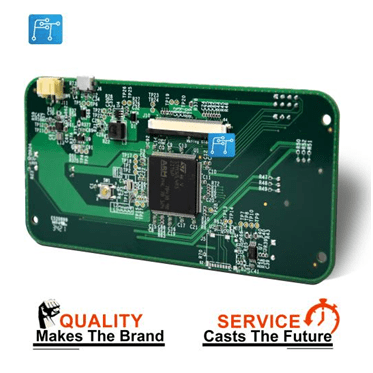
10 PCB Design Tips
1. Set the width of the traces before PCB design
Even before you start routing or laying out parts, you must know the width of your traces to accommodate the current it requires. In general, we recommend adjusting your traces to 0.01 inches for digital and analog signals with low current requirements. Also, if you are dealing with traces that can hold currents higher than 0.3 amps, set the traces wider.
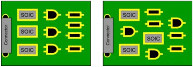
2. Careful component placement
Even before you start routing or laying out parts, you must know the width of your traces to accommodate the current it requires. In general, we recommend adjusting your traces to 0.01 inches for digital and analog signals with low current requirements. Also, if you are dealing with traces that can hold currents higher than 0.3 amps, set the traces wider.
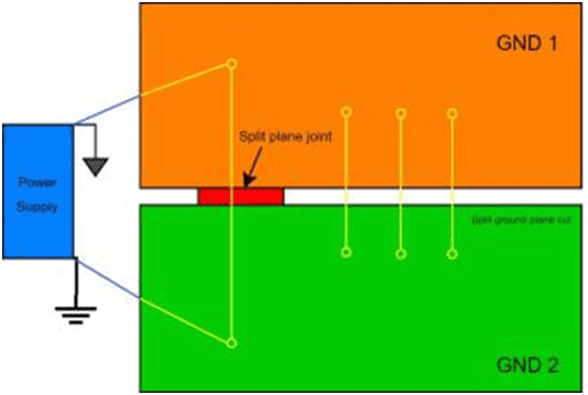
3. Set the ground plane and power plane
We recommend creating ground and power planes on the middle layers of the PCB. Placing these layers will make your board stronger and ensure it doesn’t bend during component placement.
4. Consider EMI in the circuit board
Since you may be working with high voltage PCBs, you must understand that electromagnetic interference (EMI) can damage low current and voltage control circuits. You can reduce EMI effects by separating the control and power ground planes for each stage of the power supply. If placing a ground plane between the stacks, be sure to place a path as an impedance. And remember to always consider the RF part first, because it carries high frequency signals, if you put it last, you won’t have enough room to accommodate it and your design will eventually fail.
5. Prevent the combination of lead-free and leaded components
There are many more mature parts still in use, but no lead-free options. Keep in mind that you may be tempted to put one of these into service with your latest lead-free components, please reconsider. The thermal specifications of lead and lead-free parts are significantly different, especially for RoHS certified parts.
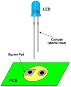
6. Create the correct silkscreen marks
We recommend identifying components on a PCB in an easy-to-follow way to understand ways to make the component placement and orientation/orientation process as easy as possible. For example, helpful symbols are included to guide the placement of the cathode and anode pins of the LEDs on the board.
7. Consider heating issues
If you’ve ever noticed that your circuit’s performance degrades over time, you probably know how much of a toll a heat dissipation problem can take in some off-the-shelf products. To help you with your thermal issues, find the parts on your board that dissipate the most heat. One of the best ways to find this information is to look up the thermal resistance rating in the datasheet and read its support guide.
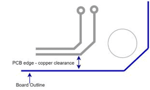
8. Leave a gap between the edge of the board and the copper
Remember to leave a small gap or gap between the edge of the board and the trace or copper plane. Set up design rules in DRC before starting the design process, such as defining board-to-edge or copper-to-edge clearances. If you want to set a gap of at least 50 mils, you should be fine. But be sure to double check with your manufacturer before ensuring their recommended clearance requirements.
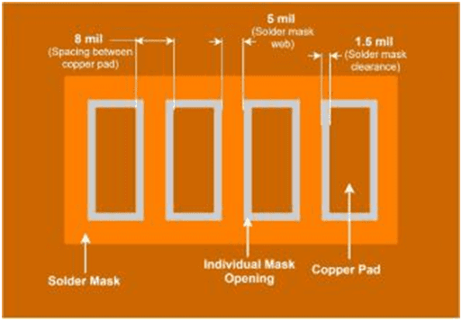
9. Please check the solder mask carefully
This usually happens when designers mistakenly ignore solder mask between pads. This is possible when the designer changes the setup from the initially larger board to the smaller board. Of course, now their pad holes are too big. In any case, when you want to send your board design to a manufacturer or supplier, double check that there is already solder mask between all pads. These tips will reduce the chance of corrosion and bridging.
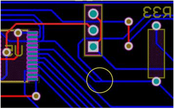
10. Please double check the acute angle
Today, most designers know how to prevent sharp angles in traces. However, they can still do this wrongly through the crack, especially if there are two joint marks. Why is this so important? Because sharp angles encourage corrosion to develop, which destroys the copper and creates defects in the circuit.
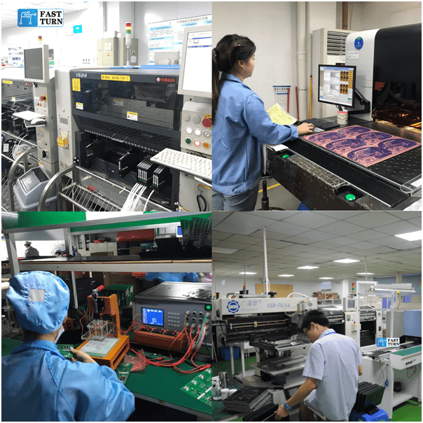
Founded in 2015, The company takes PCB sample manufacturing as the entrance, and has the ability of fast delivery of high-end samples and small and medium-sized batches. Through the whole value chain services such as PCB manufacturing, BOM purchasing and PCB assembly, we provide customers with vertically integrated one-stop solutions for their products. We continue to contribute to the continuous innovation and development of China’s electronic technology, in order to build a first-class electronic product design and manufacturing outsourcing service provider. Pursue the material and spiritual happiness of all staff and make contributions to the progress and development of mankind and society.
We offer professional design solutions covering all aspects of PCB and PCBA layout, including the following board technologies.
Include:
1.PCB design: free laminated design and impedance calculation.
2.PCB manufacturing :PCB board making capacity of 1-48 layers, blind hole, copper thickness up to 12 ounces
3. Component purchase :BOM purchase within 3 days
4.PCB assembly: urgent sample and batch assembly processing, only 1-3 days
5. Functional testing
6. Electronic assembly global logistics
7. Single, double-sided, multi-layer board
8. Rigid circuits, flexible circuits and rigid-flexible circuits.
Please email us to get a quote right away: sales@fastturnpcbs.com
Telephone number: 15018735409
