Stay Updated With The Latest Insights, Trends, And Innovations In Electronics Manufacturing. Explore Expert Articles, Industry Analysis, And Technical Guides Curated By The fastturn Team.
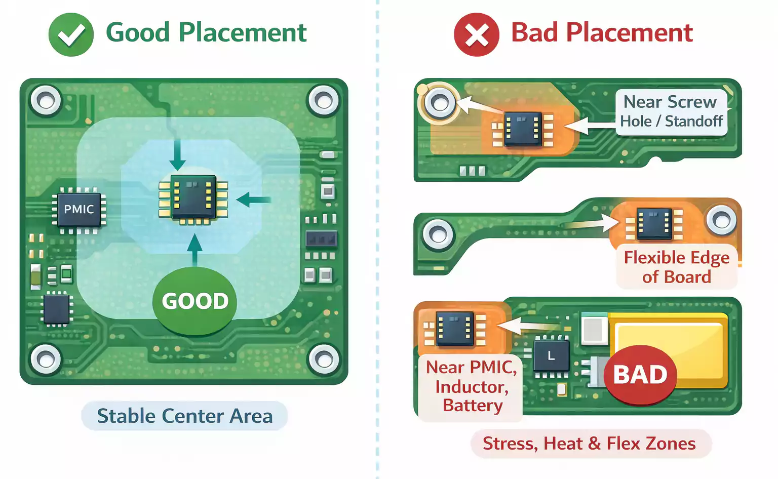
Learn the essentials of PCB accelerometer design, including sensor placement, footprint rules, routing, soldering, and validation. This guide shows how to reduce stress, heat, and vibration effects for more accurate and reliable motion sensing.
Learn what solder mask is, why it’s essential in PCB manufacturing, and how to choose the right type for your application. This in-depth guide covers materials, design rules, common defects, and reliability tips to help engineers create high-performance circuit boards.
Discover what Solder Paste Inspection (SPI) is, how 3D SPI outperforms 2D systems, and why it’s essential for boosting SMT yield, reducing defects, and enabling smart factory integration.
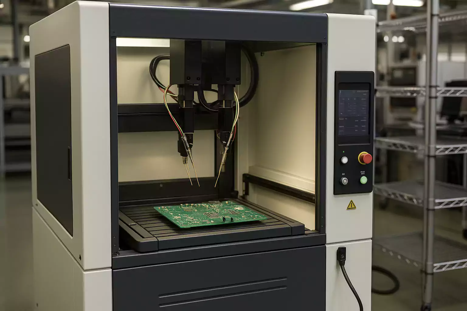
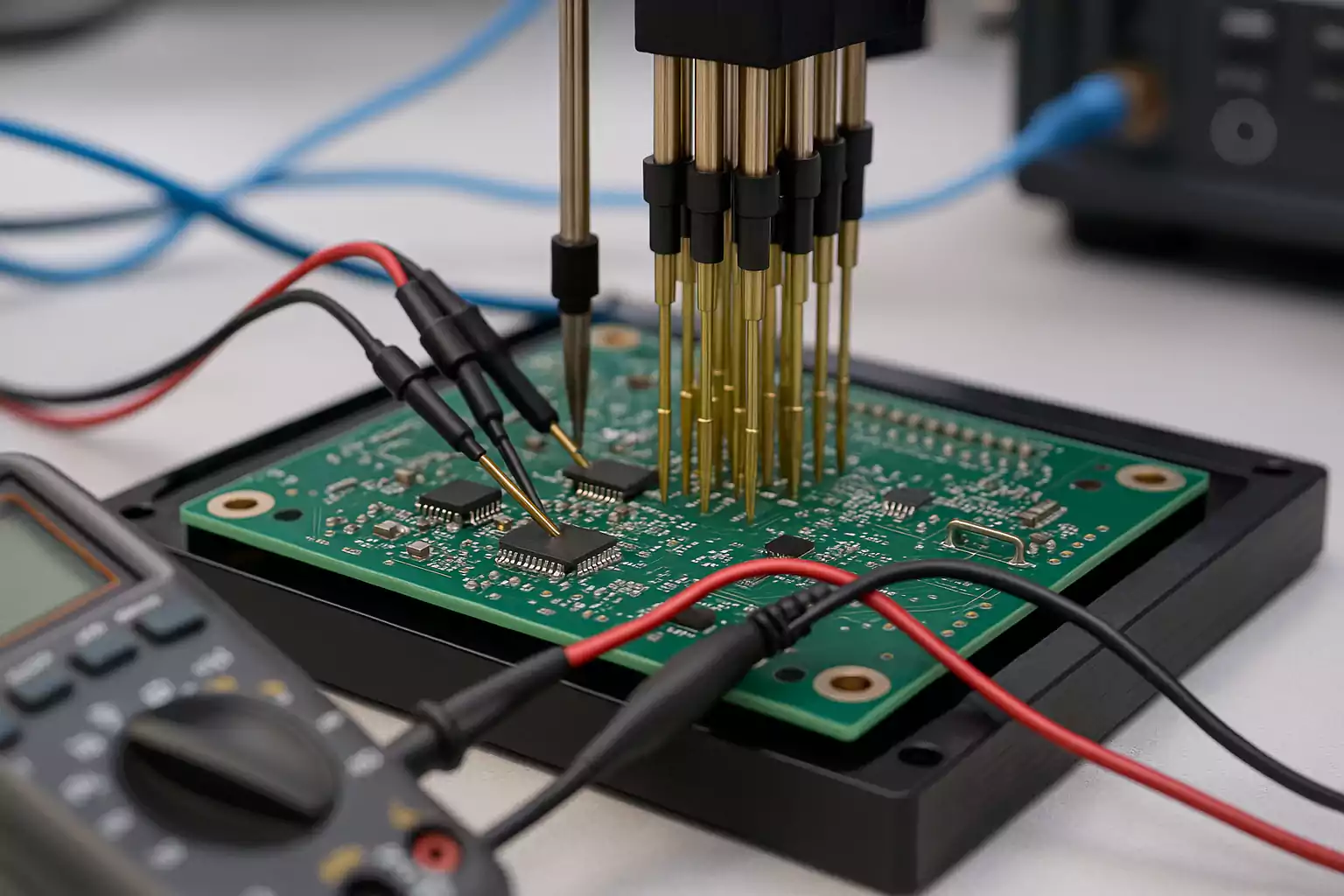
Flying Probe Testing offers a fast, fixture-free solution for prototype and low-volume PCB testing. Learn how it works, when to use it, cost benefits, design tips, and how it compares to traditional methods—all in one expert guide.
Discover how Functional Circuit Testing (FCT) ensures your PCB works before deployment. Learn its benefits, how it compares to ICT and AOI, key equipment, real-world use cases, and best practices for reliable, defect-free electronics.
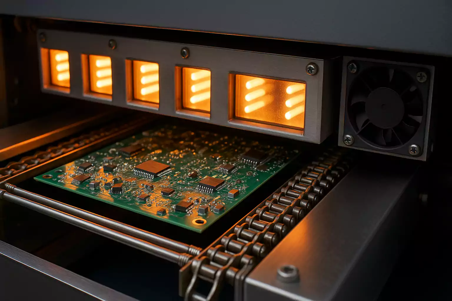
Learn everything about the reflow soldering process in SMT—from temperature profiles and oven types to common defects and best practices. This expert guide helps you master reliable, lead-free soldering and boost your PCB assembly yield.
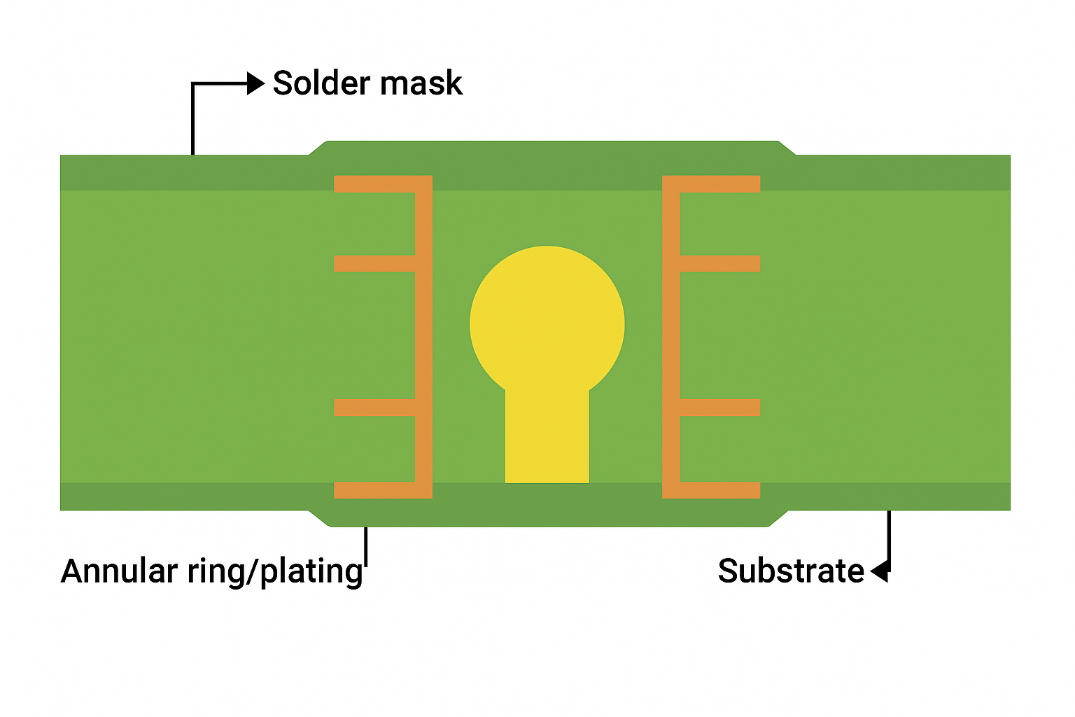
Discover how PCB plating works—from through-hole copper plating to ENIG and OSP finishes. Learn key steps, materials, and tips to improve solderability and reliability.
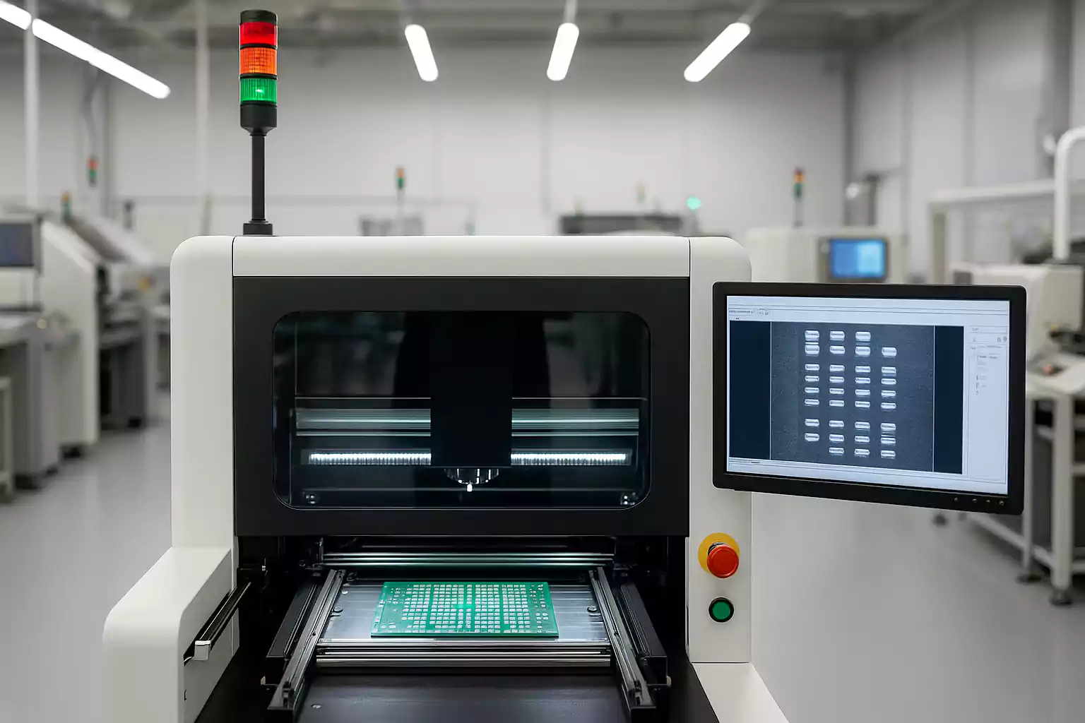
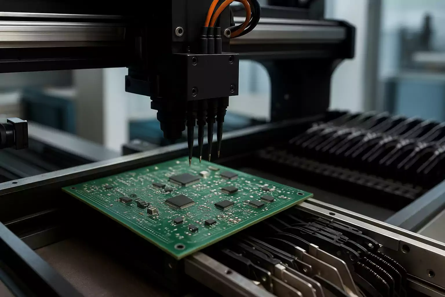
Discover how pick-and-place machines power modern PCB assembly with unmatched speed and precision. Learn key types, core features, and expert tips to choose and optimize the right SMT solution for your production needs.
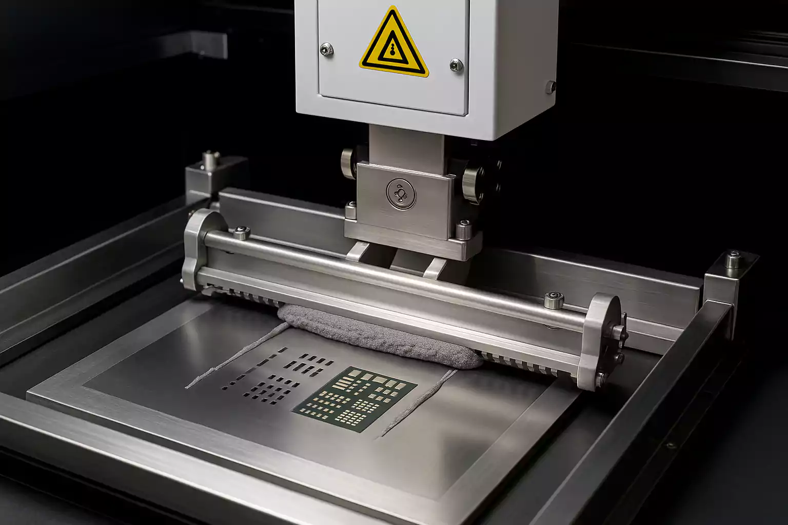
A complete guide to solder paste stencil printing in SMT assembly. Learn stencil design, print parameters, defect control, and best practices for high-yield PCBs.
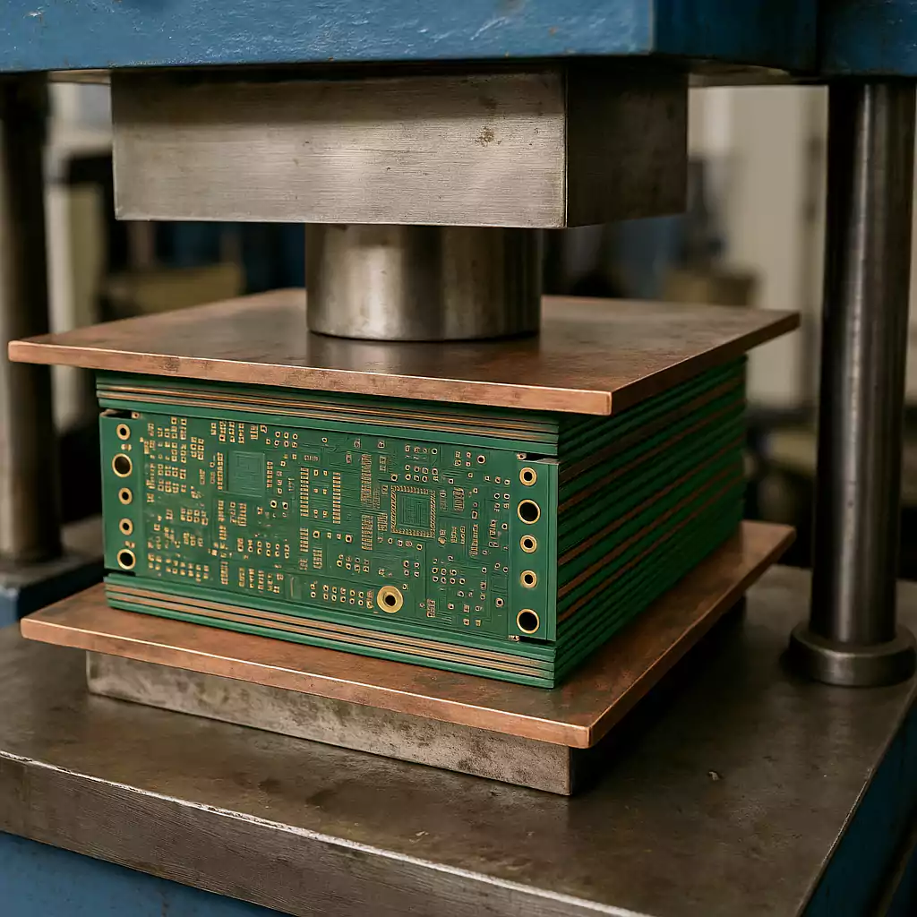
Learn how multilayer PCBs are bonded through the lamination process and discover expert tips to avoid delamination. This complete guide covers materials, process steps, and reliability best practices for high-performance PCB fabrication.