Stay Updated With The Latest Insights, Trends, And Innovations In Electronics Manufacturing. Explore Expert Articles, Industry Analysis, And Technical Guides Curated By The fastturn Team.
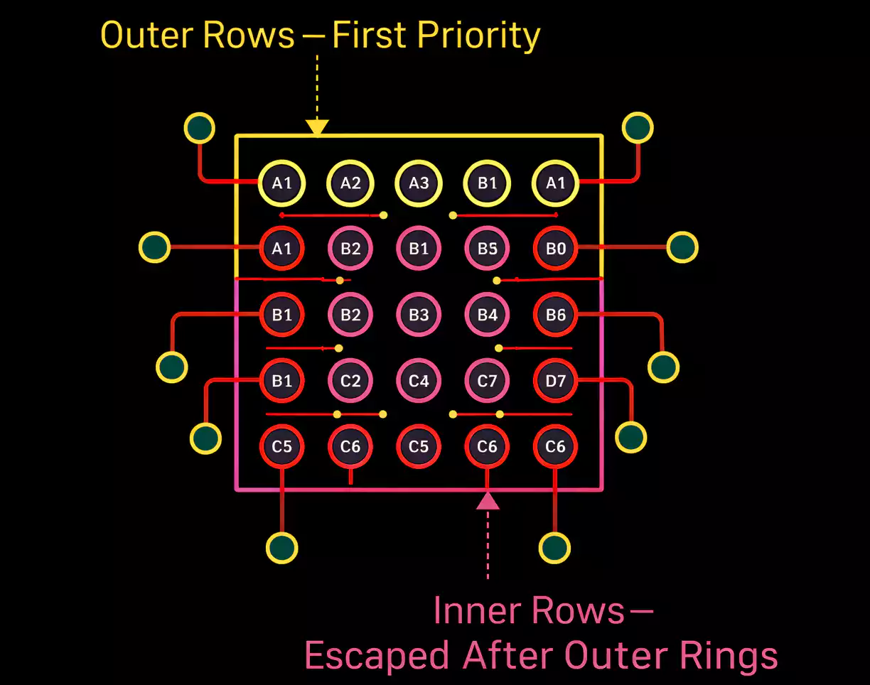
Learn how to design a reliable BGA PCB board with proven best practices for placement, fanout, routing, stack-up, and DFM—avoid re-spins and assembly failures.
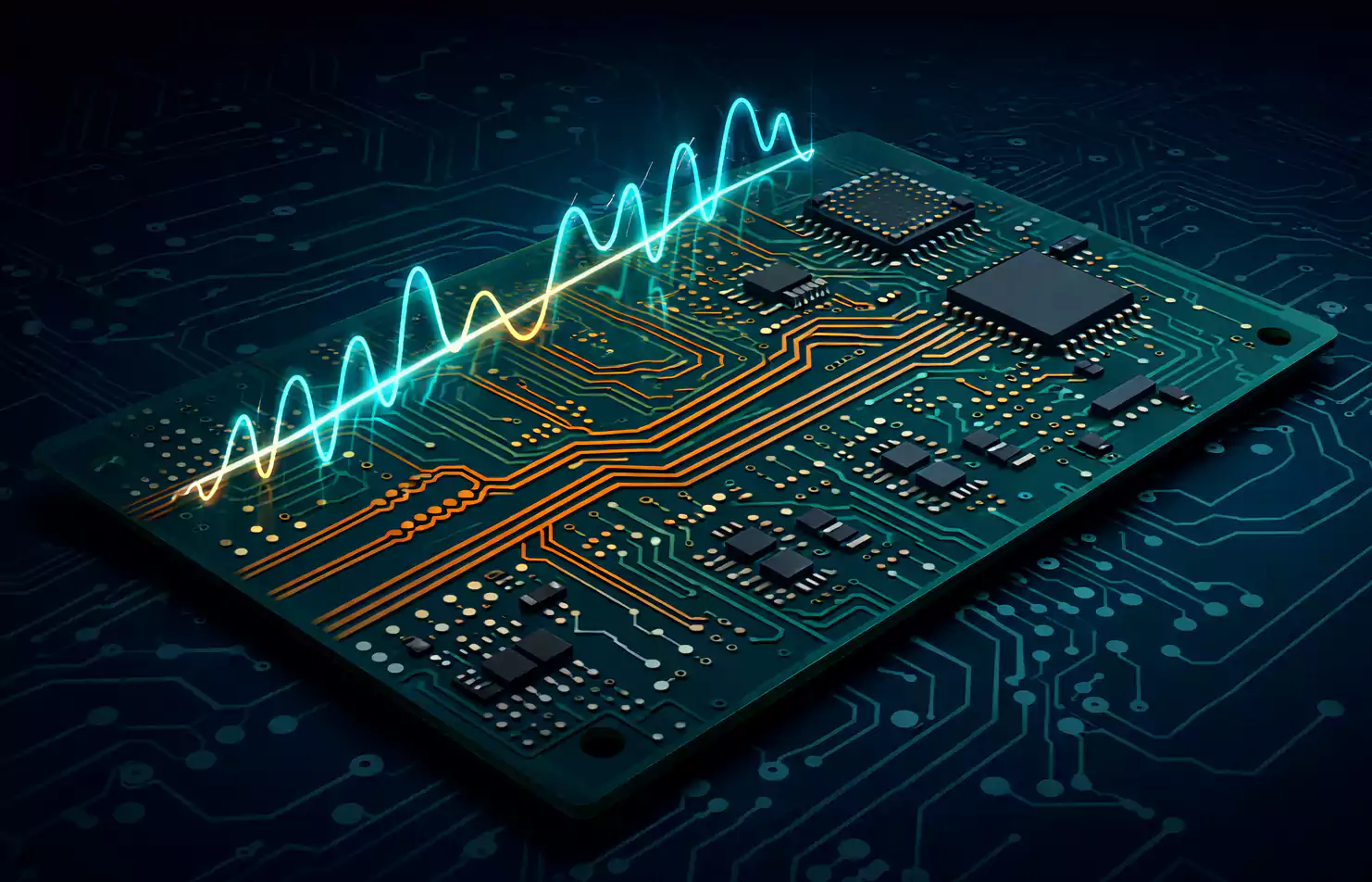
Learn a proven high-speed PCB design flow covering placement, routing constraints, signal integrity, timing analysis, routability checks, and manufacturing files—so your boards work on the first spin.
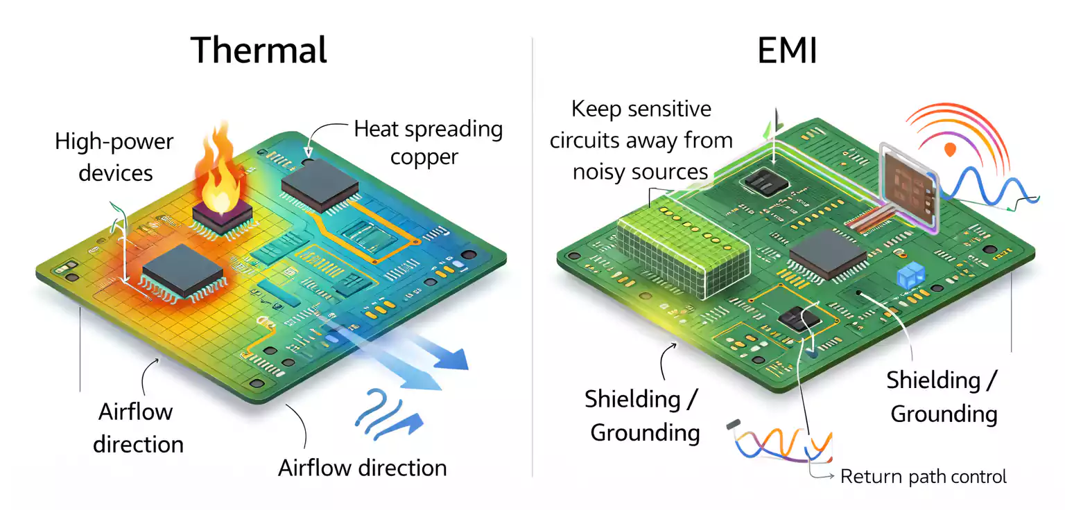
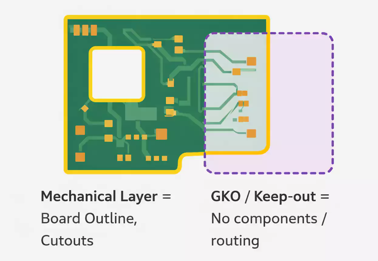
Learn the modern PCB design flow—from system specs and block diagrams to simulation, PCB layout guidelines, component placement, thermal management and EMI best practices.
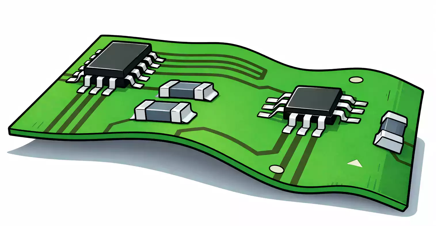
Learn what board warpage (PCB warpage) is, why it ruins component alignment and yield, the acceptable limits, and 9 proven design and process fixes to keep your PCBs flat.
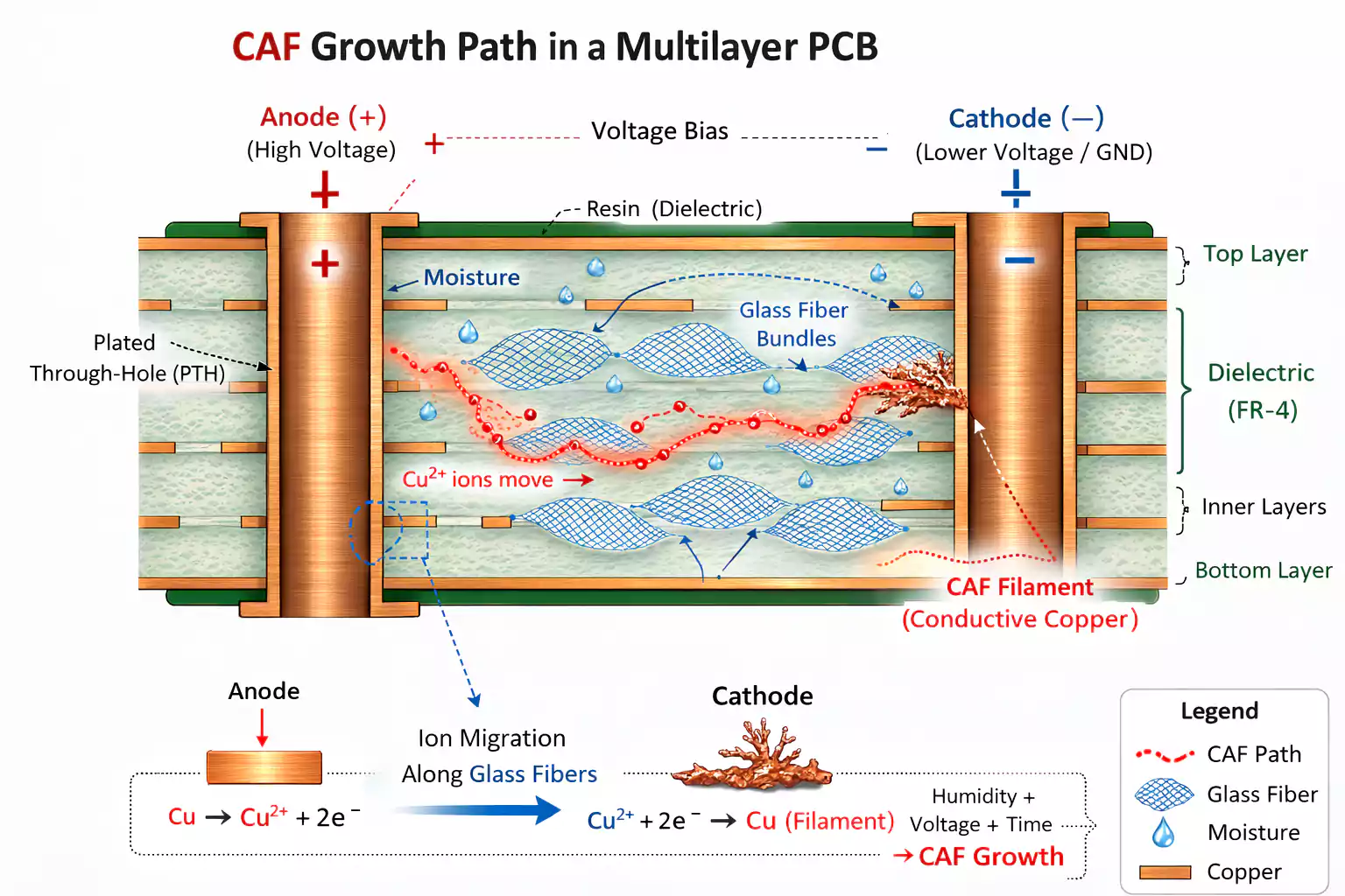
Learn what Conductive Anodic Filament (CAF) is, why it causes hidden PCB failures, and how smart layout, spacing, and materials can prevent CAF and boost long-term reliability.
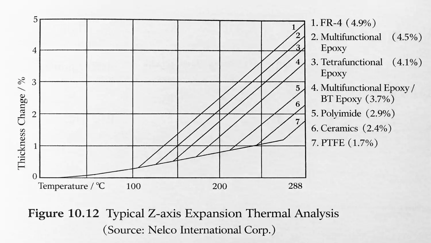
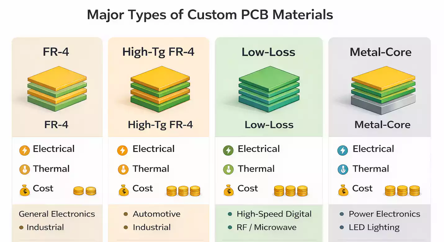
Choose the right PCB board material—FR-4, polyimide, ceramics, PTFE, and embedded passives—to maximize reliability, signal integrity, thermal performance, and manufacturability.
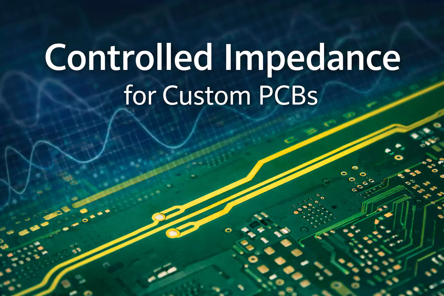
Learn when controlled impedance is required for custom PCBs, step-by-step design & routing best practices, and exactly what to specify to your PCB manufacturer.
Custom PCB Material Selection Guide: Learn how to choose FR-4, High-Tg, low-loss, or metal-core laminates to optimize signal integrity, thermal performance, manufacturability, and cost.