

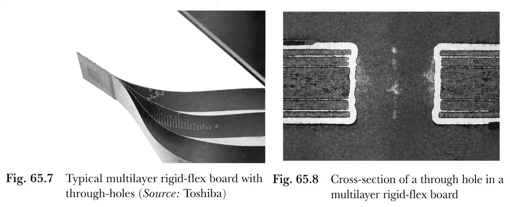
Rigid flex PCB manufacturing combines flexible polyimide layers with rigid FR-4 sections in one integrated structure. Unlike a standard rigid board or a simple flex-to-board connection, a true rigid-flex build requires a multi-step fabrication process that must control both mechanical support and bendability at the same time.
The rigid flex PCB manufacturing process typically includes inner flex circuit formation, lamination, drilling, desmear, plating, coverlay application, and controlled routing or deep milling to expose the flex areas. Each step affects how well the finished board handles interconnection reliability, bend performance, thickness control, and final assembly.
That is why rigid flex PCB fabrication is more demanding than standard multilayer PCB fabrication. Success depends on how well the manufacturer manages material transitions, hole quality, bend-zone protection, and process consistency across the entire build.
Quick Answer: What Is the Rigid Flex PCB Manufacturing Process?
A typical rigid-flex PCB manufacturing process includes:
- Building the flex core
- Forming conductor patterns
- Applying coverlay and pre-opened bondply
- Machining the rigid outer sections
- Laminating the rigid and flex sections together
- Drilling and desmearing the holes
- Plating through-holes or vias
- Imaging and etching outer layers
- Applying surface finish
- Final routing and forming
What makes this process different is not simply the number of steps. The real challenge is protecting bend areas, controlling the rigid-to-flex transition, and maintaining reliability through lamination, drilling, desmear, and plating.
Why the Rigid Flex PCB Fabrication Process Is More Complex
A standard multilayer rigid PCB already requires tight control over:
- lamination
- drilling
- plating
- imaging
- surface finishing
The rigid-flex PCB fabrication process adds another layer of complexity because it must also account for:
- bend-area protection
- rigid-to-flex transitions
- uneven panel support during lamination
- moisture control
- dimensional movement through repeated heat cycles
- final release of the flex sections
In practice, the challenge is not that there are simply more steps. It is that nearly every step must work for both rigid and flexible regions at the same time.
That is why rigid-flex design should begin with a realistic understanding of manufacturing capability. A supplier may be strong in rigid multilayer boards or flexible circuits, but rigid-flex PCB manufacturing requires both skill sets in one coordinated process.
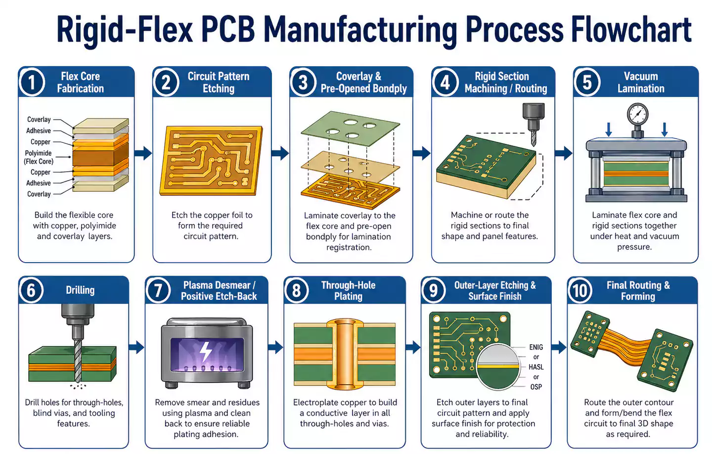
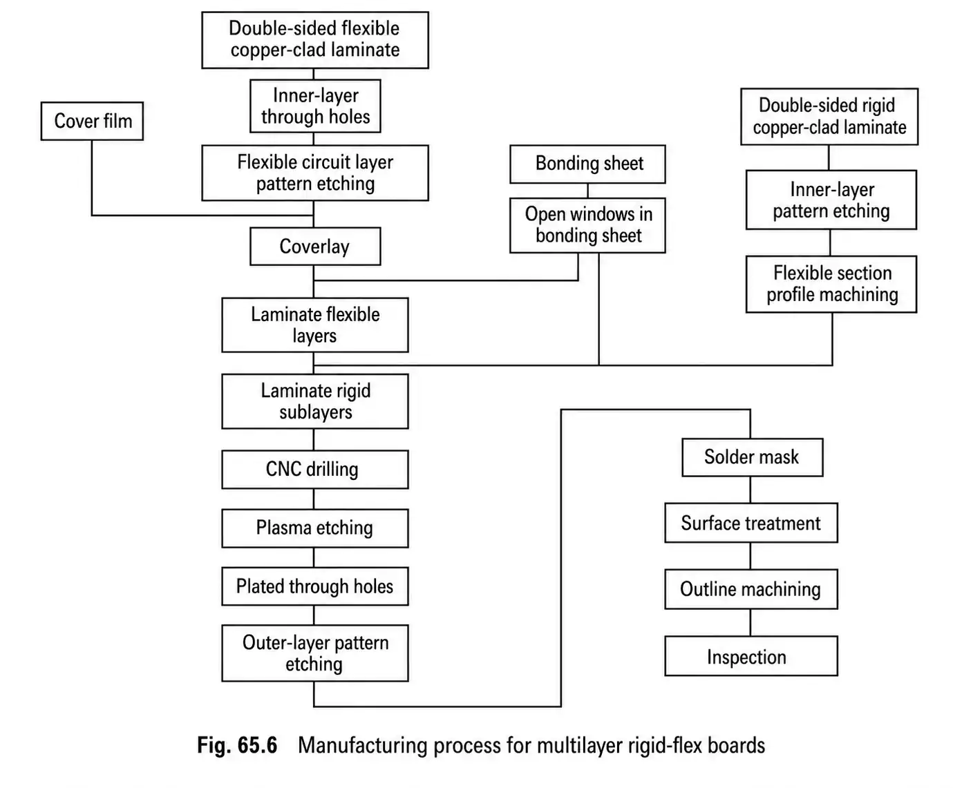
Typical Rigid Flex PCB Manufacturing Process
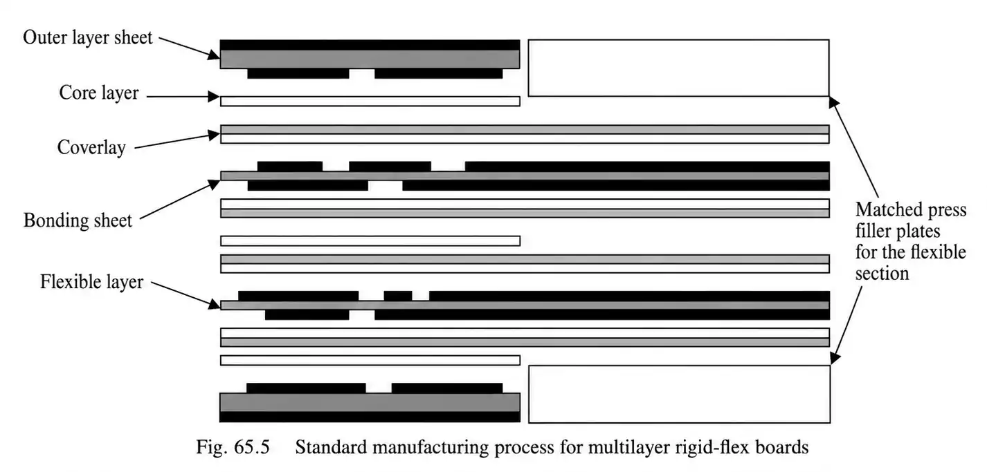
1. Start With Double-Sided Flexible Copper-Clad Laminate
A common rigid-flex PCB manufacturing process begins with double-sided flexible copper-clad laminate.
With the exception of plated through-holes, conductor patterns are typically formed first by conventional etching. This establishes the flex core circuitry before the rigid sections are added.
2. Protect the Flex Areas
In the flex sections, the conductors are covered with coverlay that has no openings in the bend region.
Between multiple flexible layers, bondplies are pre-opened in the flex zones so the adhesive does not interfere with bending later. This is one of the most important design-for-manufacturing details in a reliable rigid-flex build.
3. Machine the Rigid Outer Sections
The rigid outer sections are usually made from double-sided rigid copper-clad material.
Before final lamination, the rigid material in the flex region is processed using:
- CNC routing
- punching
- laser machining
Depending on the design, the rigid material in the flex zone may be:
- fully removed
- partially depth-routed
This step creates the physical transition between the rigid sections and the flexible sections. It is also why rigid-flex PCB routing is more specialized than standard profile routing.
4. Laminate the Structure
After the rigid outer layers are prepared, they are bonded to the flex structure using bondply that has already been opened in the flex area.
If the rigid section is routed out over the flex area, the flex region needs a support fill plate or similar pressure-support insert during lamination.
Rigid-flex PCB lamination is especially important because pressure must remain uniform across areas with very different thicknesses and support conditions. Vacuum lamination is often preferred because it provides more even pressure across the panel. Assist materials such as PE film can also help the bondply flow and fill gaps more completely, especially in more complex structures.
5. Bake Before Critical Steps
Before bonding or lamination, baking is commonly used to remove absorbed moisture.
That moisture control matters because flexible materials, bondplies, and coverlays are more sensitive to absorbed humidity than standard rigid materials. If moisture is not removed early, it can affect later lamination quality, rigid-flex PCB drilling, and hole-wall treatment.
6. Drill and Desmear the Holes
After lamination, the panel moves into rigid-flex PCB drilling and through-hole processing.
At this stage, the flow begins to resemble standard multilayer PCB fabrication, but the rigid-flex PCB desmear process becomes a major point of difference. After proper baking, the holes are drilled and plasma etching is used to remove resin residue from the hole walls. Baking before plasma treatment is also important.
The recommended etch-back depth is generally around 13 µm or less.
7. Plate the Through-Holes
Standard plated through-hole processing can be used after desmear, but rigid-flex PCB plating parameters should be based on through-hole reliability testing, not simply copied from rigid-board practice.
8. Finish the Outer Layers and Final Form
The remainder of the rigid-flex PCB fabrication process becomes more familiar:
- outer-layer imaging and etching
- coverlay or solder mask
- surface finish
- routing and profile processing
In the final forming step, the support material or depth-controlled rigid cap is removed from the flex region, leaving the finished rigid-flex structure.
Rigid Flex PCB Manufacturing Process Summary
| Flex core fabrication | Build the base circuitry | Starts with flexible copper-clad laminate instead of a full rigid stack |
| Coverlay and bondply prep | Protect conductors and preserve bendability | Flex zones require no-opening coverlay and pre-opened bondply |
| Rigid section machining | Create rigid-to-flex transitions | Requires routing, punching, or laser depth control in flex areas |
| Lamination | Bond rigid and flex sections together | Needs fill plates, vacuum lamination, and uniform pressure support |
| Drilling | Form plated holes | Drill parameters must match material and structure, not just thickness |
| Desmear | Remove resin residue | Plasma desmear is often preferred over permanganate |
| Plating | Build reliable conductive hole walls | Must be tuned for reliability, especially in high-stress applications |
| Final forming | Release the finished structure | Flex zones must be opened cleanly without edge damage |
Why Through-Hole Processing Is a Critical Reliability Point
If the flexible inner layers include through-holes, those metallized holes are formed early, before inner-layer etching, much like rigid inner-layer processing.
The drilling equipment can be similar to what is used for rigid boards, but the rigid-flex PCB drilling parameters cannot simply be reused. Factors that affect the drilling window include:
- material type
- adhesive system
- layer construction
- support conditions in rigid and flex areas
Baking before drilling is also a key step in producing reliable plated through-holes.
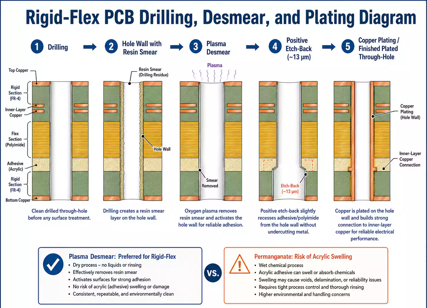
Why Plasma Desmear Is Often Preferred
Potassium permanganate is widely used in rigid PCB processing, but it can be problematic in rigid-flex boards, especially when acrylic adhesive systems are present.
Acrylic materials may swell significantly in permanganate, which can reduce hole reliability. Because of that, rigid-flex PCB desmear is often done with plasma instead.
Copper Thickness Still Matters
For high-reliability applications such as aerospace and industrial electronics, hole wall copper requirements are more demanding.
Typical recommendations include:
- more than 25 µm of hole wall copper for high-reliability environments
- more than 35 µm under certain IPC-6013C-related conditions
Consumer products may accept thinner copper, but that changes the reliability balance rather than removing the reliability challenge.
Positive Etch-Back and Why It Matters
Plasma treatment can also be extended into a positive etch-back process, with a commonly recommended depth of about 13 µm.
This helps by:
- removing resin residue
- etching back adhesive and polyimide without attacking metal
- cleaning the metal surface
- improving copper connection to the inner-layer target during plating
Reliable holes are not only about copper thickness. They also depend on surface condition and how well the plated copper ties into the inner-layer copper structure.
How Material Selection Affects the Rigid Flex PCB Manufacturing Process
Material choice directly affects process stability and long-term reliability.
High-Reliability Builds
For aerospace and military-type builds, thicker polyimide film, generally over 50 µm, is preferred because it offers better process stability and durability.
Consumer Electronics Builds
Consumer electronics usually move toward thinner dielectrics, below 50 µm, to support lighter and thinner products.
Adhesive Tradeoffs
Different adhesive systems behave differently:
- Acrylic adhesives: stronger bond strength, but lower heat resistance and higher shrinkage
- Epoxy adhesives: better heat resistance, but longer cure times and somewhat lower bond strength
Why Adhesiveless Materials Matter
Adhesiveless copper-clad laminates are especially attractive because they typically offer:
- better heat resistance
- lower coefficient of thermal expansion
- reduced final thickness
These benefits become even more important in thin, high-density, or thermally demanding builds.
High-Temperature Coverlay and Bondply
Modern hot-melt polyimide coverlays and bondplies can reduce drilling smear and improve reliability, but they may require processing temperatures above 300°C. That raises both equipment requirements and process-control demands.
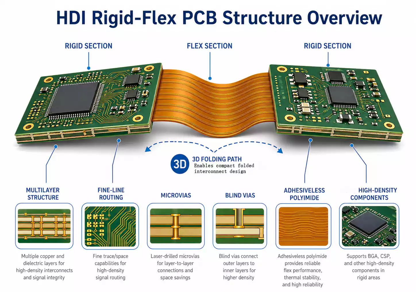
HDI Rigid-Flex PCB Fabrication: Sequential Build-Up, Blind Vias, and Laser Processing
High-density rigid-flex boards follow a different path from traditional high-reliability aerospace-style constructions.
Industrial and medical products increasingly use rigid-flex designs that combine high density with high reliability. Typical HDI rigid-flex characteristics include:
- line pitch below 100 µm
- hole diameters below 100 µm
- 25 µm or thinner adhesiveless thin-copper polyimide laminates
- copper thickness around 18 µm or less
- laser-drilled microvias, especially blind vias
For these designs, sequential build-up processing has become a standard route. This part of the rigid-flex PCB fabrication process often includes blind vias smaller than 100 µm formed by CO2 laser drilling and then plated with a thin copper layer.
As routing density increases and the board gets thinner, rigid-flex PCB manufacturing begins to overlap more with HDI manufacturing.
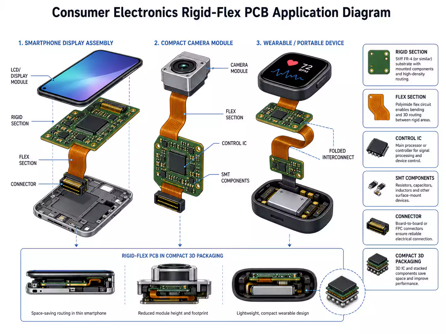
Consumer Electronics Rigid-Flex PCB Manufacturing: Density, Cost, and Throughput
Consumer devices such as smartphones and digital cameras drive rigid-flex production in a different direction.
The goal is not just compact routing. It is also:
- low cost
- high production volume
- thin profile
- efficient manufacturing
Typical consumer rigid-flex designs may include:
- line widths below 75 µm
- blind via diameters below 150 µm
- high-density SMT assembly
- many small chips mounted on rigid sections
Process Choices for Consumer Builds
To support those goals, manufacturers may use:
- buried vias or internal microvia structures
- adhesiveless materials for better thermal performance
- heat-resistant epoxy bondply in build-up processing
- CO2 laser drilling for blind vias
When copper windows are opened in advance on buildup outer layers, the laser drilling rate can increase dramatically. In the best case, a CO2 laser can produce 10,000 blind vias in one minute.
Throughput vs. Precision
If the inner layers do not contain holes, roll-to-roll processing can greatly improve productivity. If they do contain holes, using an RTR flow requires much tighter dimensional control.
For profiling, semi-automatic punching and stamping equipment can outperform CNC routing in some operations. Stainless steel punching dies can be effective, but die geometry must be carefully designed to avoid cracks or nicks at the flex edges.
Why Dimensional Control Drives Yield
Even when high-stability adhesiveless materials are used, thin flexible materials can still deform through repeated thermal cycles.
That means manufacturers need to:
- evaluate dimensional movement at each process step
- build compensation into the flow
- choose panel sizes carefully to improve yield
In high-volume rigid-flex production, dimensional compensation can be just as important as the equipment itself.
FAQ: Rigid Flex PCB Manufacturing Process
What is the biggest difference between rigid-flex PCB fabrication and standard multilayer PCB fabrication?
Rigid-flex fabrication must control both rigid and flexible regions in one integrated process. Lamination, routing, desmear, dimensional control, and final forming all have to be adapted around the rigid-to-flex transition.
Where does a typical rigid-flex manufacturing flow begin?
A common flow begins with double-sided flexible copper-clad laminate. From there, the conductor patterns are formed, coverlay and pre-opened bondplies are added, and the rigid outer sections are built into the structure.
Why are no-opening coverlays and pre-opened bondplies used in flex areas?
Because the bend region must remain flexible. If adhesive or structural material extends into the area that needs to bend, flex performance and bend life can suffer.
Why is plasma desmear often preferred in rigid-flex boards?
Because acrylic adhesive systems can swell significantly in permanganate solutions, which can hurt plated-hole reliability. Plasma desmear is generally more compatible with rigid-flex material systems.
What is positive etch-back, and why does it matter?
Positive etch-back is an added plasma-etch step, commonly around 13 µm, that improves resin removal and surface preparation without attacking the metal layers. It helps create a more reliable plated connection to the inner-layer copper.
Why do high-density rigid-flex boards use sequential build-up and laser blind vias?
Because when line pitch gets smaller, holes get smaller, and the board gets thinner, traditional through-hole routing space becomes limited. Sequential build-up and laser blind vias open up more routing density and support compact, high-function designs.
Final Takeaway
A reliable rigid flex PCB manufacturing process depends on more than completing the right steps in sequence. It depends on controlling how materials, lamination, drilling, desmear, plating, bend-zone design, and dimensional stability work together across the entire build.
Some designs prioritize thicker copper and long-term reliability. Others prioritize thinner materials, blind vias, and manufacturing efficiency. In either case, consistent results come from process control, not from any single step alone.
For complex rigid-flex projects, early collaboration with an experienced fabrication partner can help reduce risk and improve build consistency. FastTurn PCB supports that process with practical manufacturing insight from stackup planning through final production.
