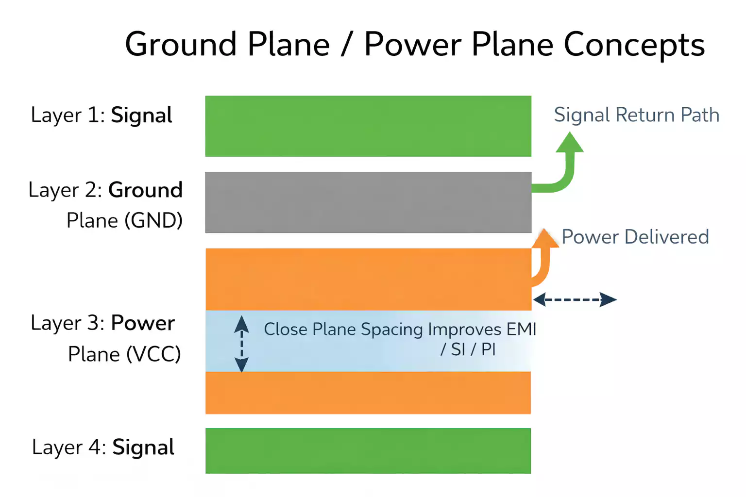
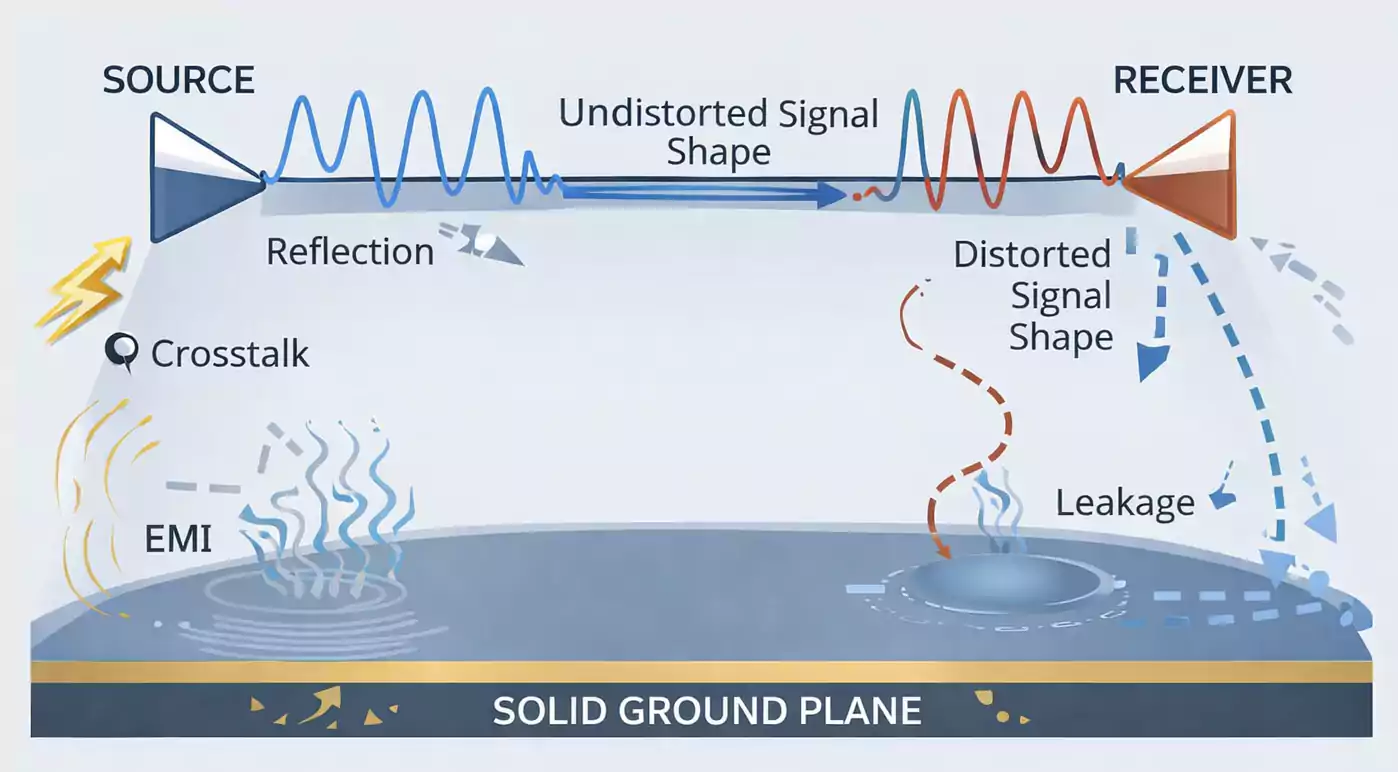
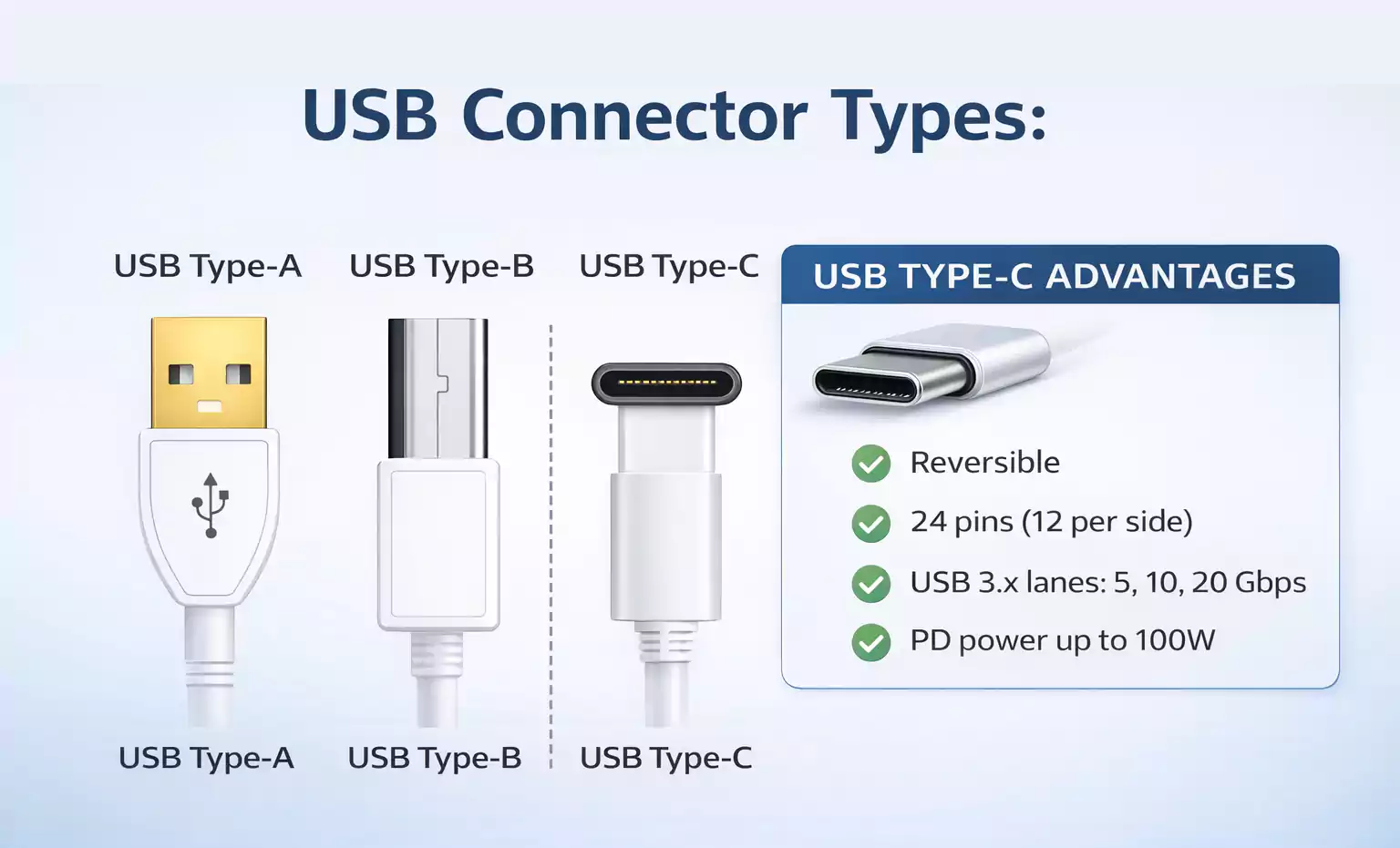
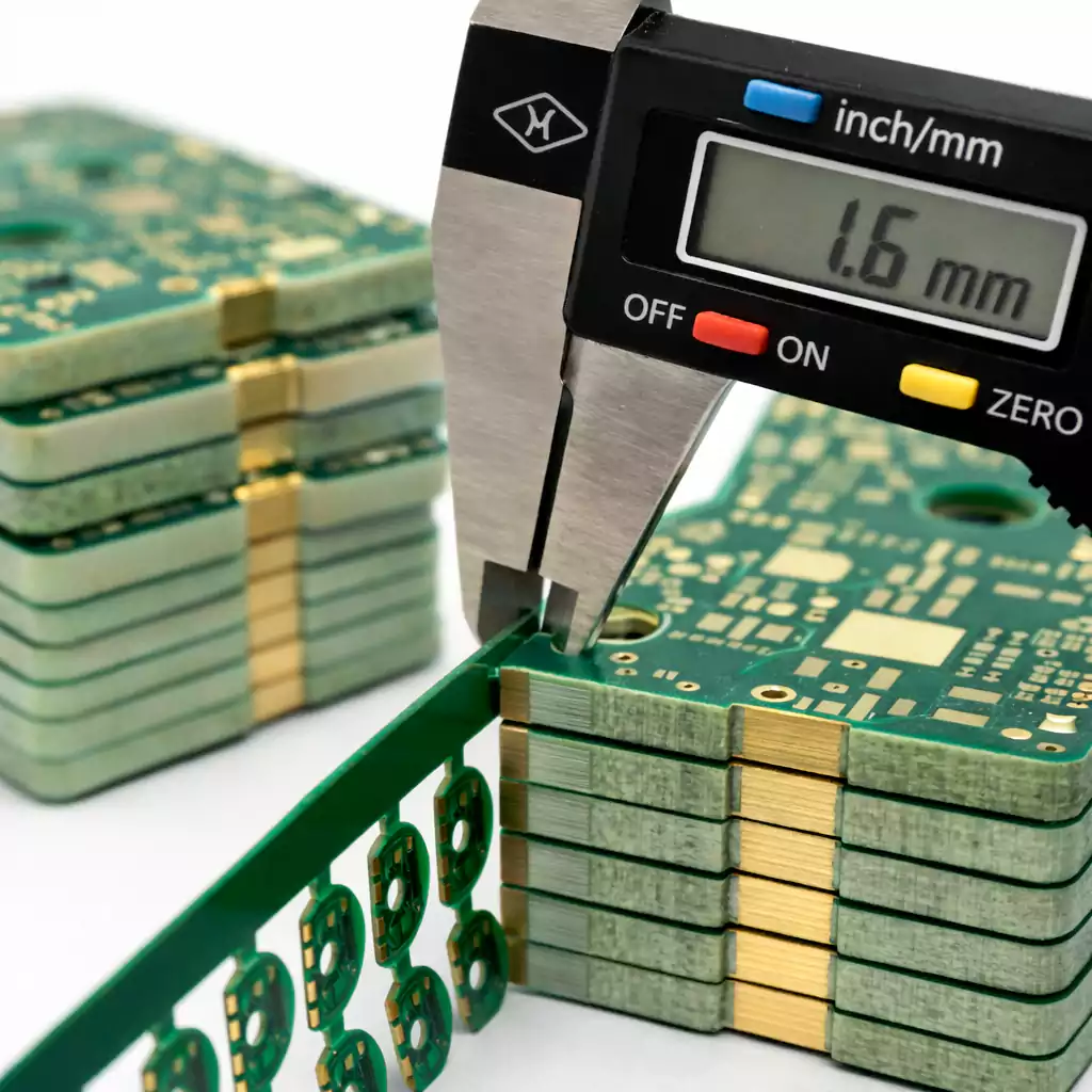
Learn why fiducial PCB marks matter and how to place global vs local fiducials, choose sizes, and improve SMT alignment, solder printing, and board testing.
Learn how to design PCB board in 10 easy steps — from schematic and stackup to PCB artwork (Gerber) and layout tips for reliable, manufacturable boards.
Heavy Copper PCB (2–20oz): boost power handling, cooling, and reliability. Get clear design tips, current-capacity guidance, and manufacturer capabilities for high-current builds.
HDI circuit boards: microvias, stack-ups, and via-in-pad explained — learn how to pick the right HDI PCB manufacturer for prototyping and mass production.
Create a production-ready pcb schematic — from symbols and netlists to Gerber export and PCBA handoff. Follow a clear step-by-step checklist and grab downloadable templates.
PCB Trace Guide: Learn how to size trace width for current and temperature, control impedance for high-speed signals, and validate designs with trace width calculators.
Learn how copper foil roughness drives GHz signal loss in high-speed PCBs. Clear skin-effect primer, Df test highlights, and practical fixes—use low-profile or RTF foils to cut insertion loss.
Discover 3 HDI strategies—fine-line etching, extra layers, and microvias—to increase PCB wiring density while maintaining yield and high-frequency performance.