HDI circuit boards: microvias, stack-ups, and via-in-pad explained — learn how to pick the right HDI PCB manufacturer for prototyping and mass production.
Create a production-ready pcb schematic — from symbols and netlists to Gerber export and PCBA handoff. Follow a clear step-by-step checklist and grab downloadable templates.
PCB Trace Guide: Learn how to size trace width for current and temperature, control impedance for high-speed signals, and validate designs with trace width calculators.
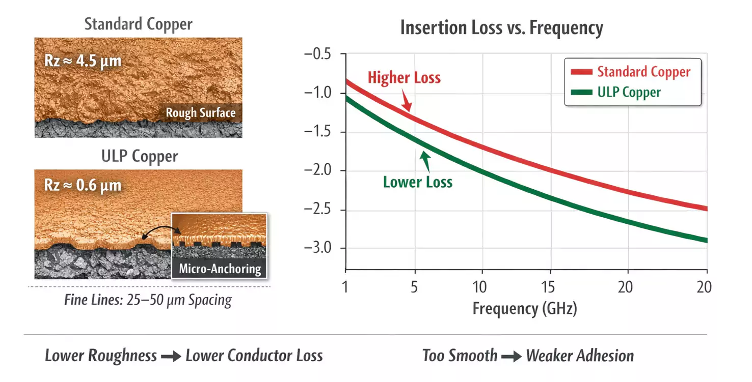
Learn how copper foil roughness drives GHz signal loss in high-speed PCBs. Clear skin-effect primer, Df test highlights, and practical fixes—use low-profile or RTF foils to cut insertion loss.
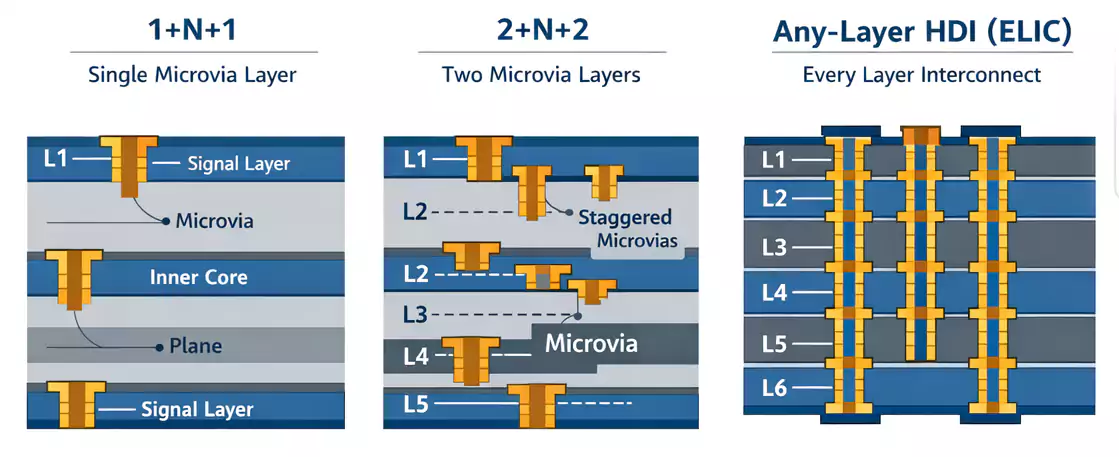
Discover 3 HDI strategies—fine-line etching, extra layers, and microvias—to increase PCB wiring density while maintaining yield and high-frequency performance.
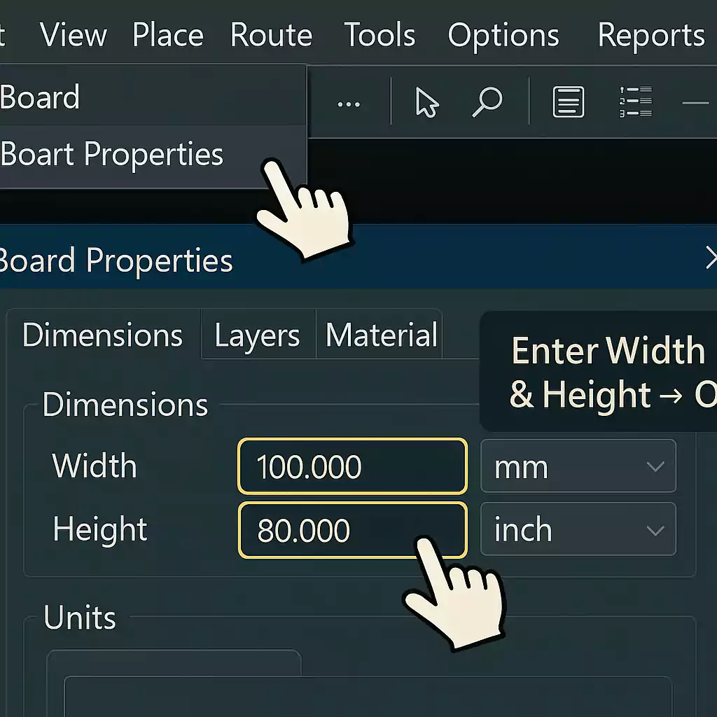
How to Change PCB Board Size in Ultiboard: 4 easy methods — numeric edit, drag-resize, DXF import or redraw — plus a quick checklist to avoid fabrication errors.
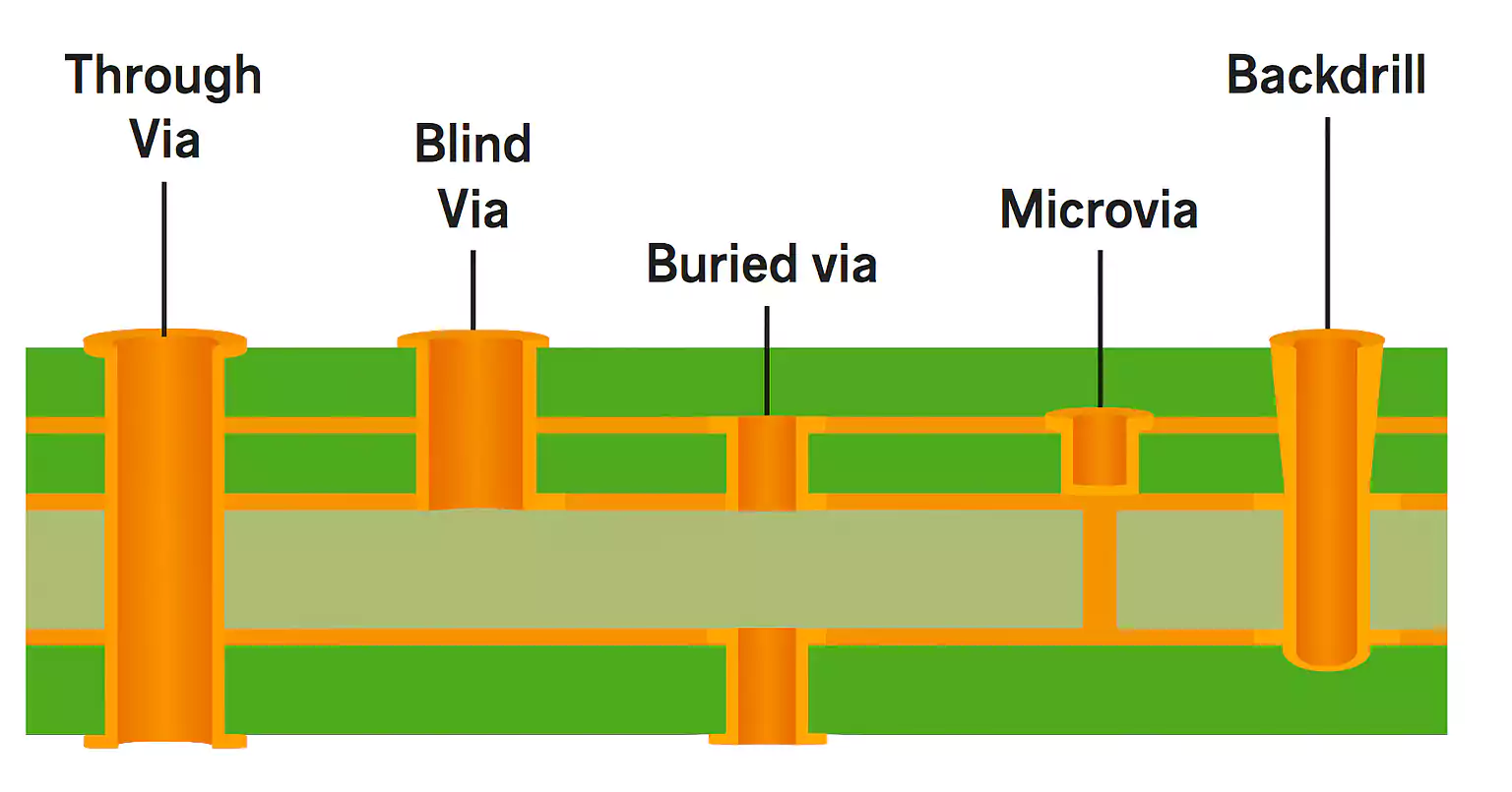
Quickly master PCB via design: types, sizing, aspect ratio, tenting & reliability — practical tips to avoid manufacturing mistakes and speed up your HDI builds in 2025.
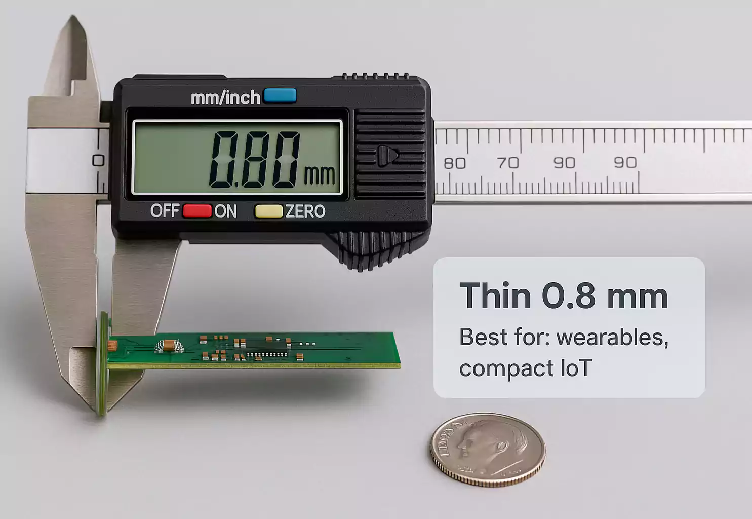
PCB Printer & Thickness Guide — how PCB printers pick standard PCB thicknesses, tolerances, and stack-ups. Clear 3-step method, quick chart, and ordering checklist to get perfect boards.
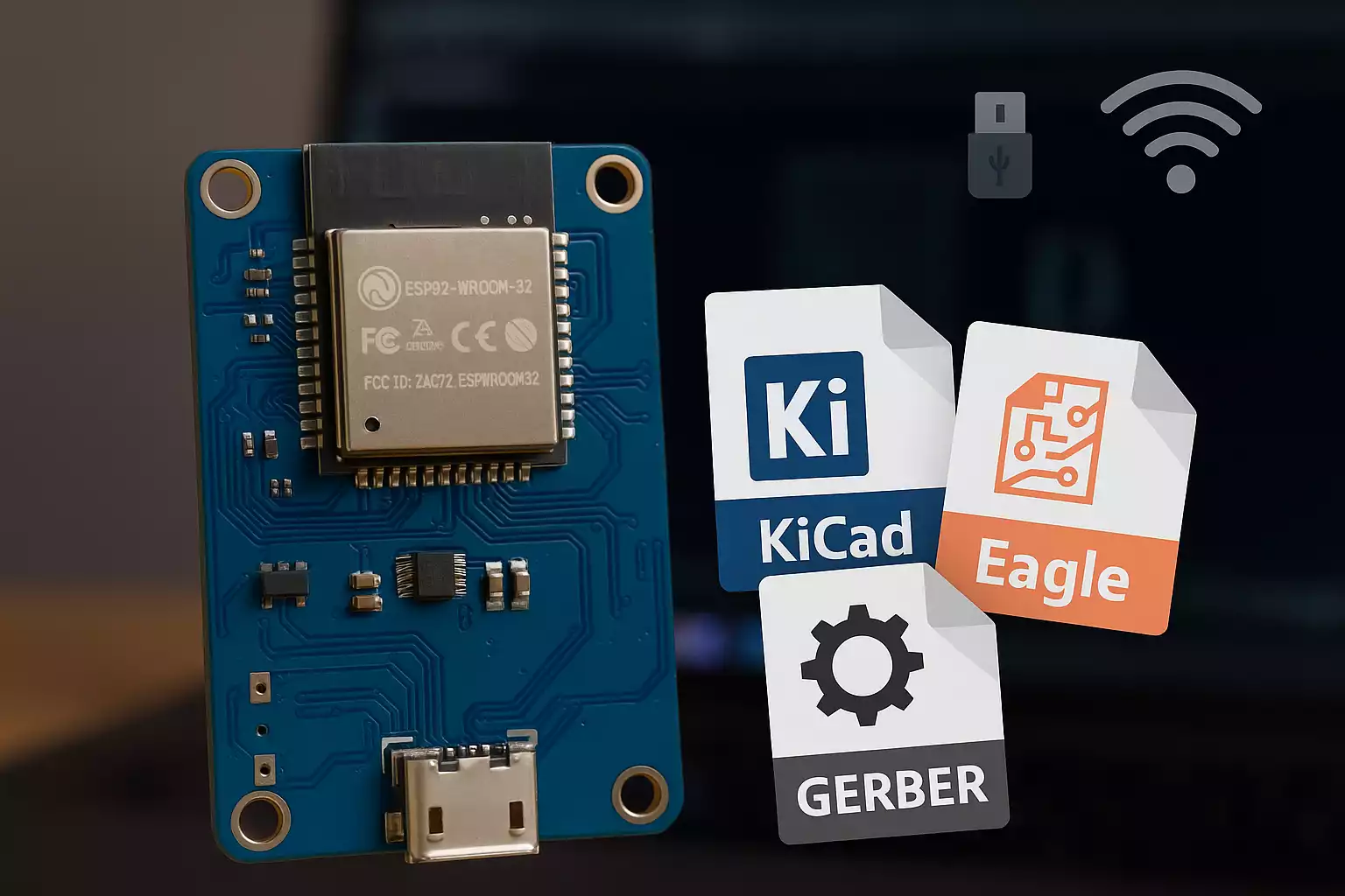
Get trusted esp32 pcb file downloads — official Espressif reference layouts, open-source KiCad/Eagle projects, and ready-to-order Gerbers, plus a simple edit-and-order guide.