Stay Updated With The Latest Insights, Trends, And Innovations In Electronics Manufacturing. Explore Expert Articles, Industry Analysis, And Technical Guides Curated By The fastturn Team.
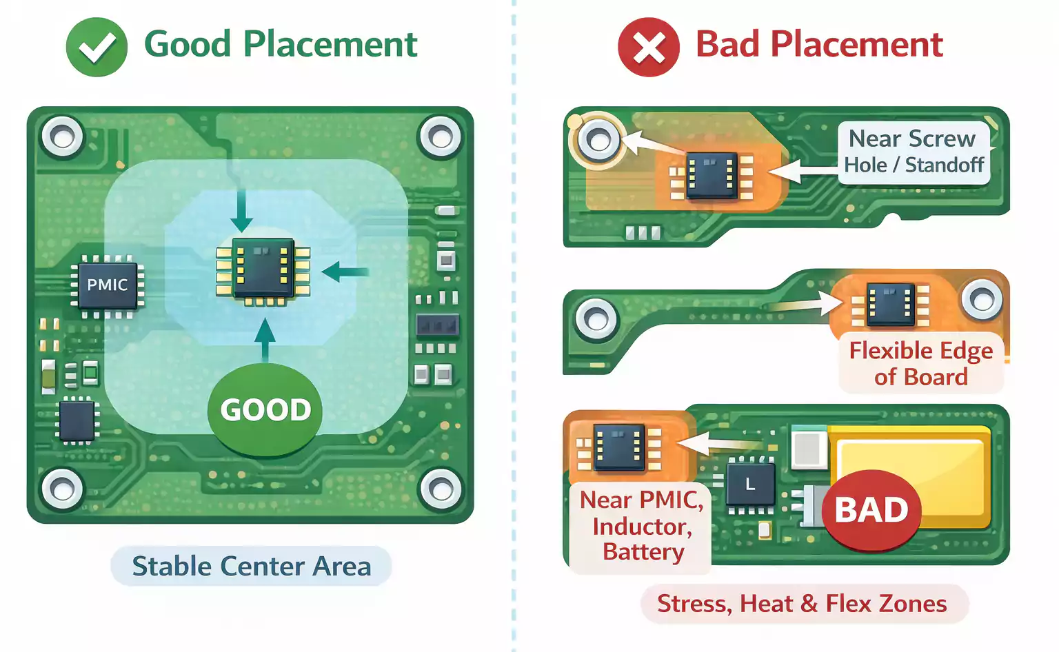
Learn the essentials of PCB accelerometer design, including sensor placement, footprint rules, routing, soldering, and validation. This guide shows how to reduce stress, heat, and vibration effects for more accurate and reliable motion sensing.
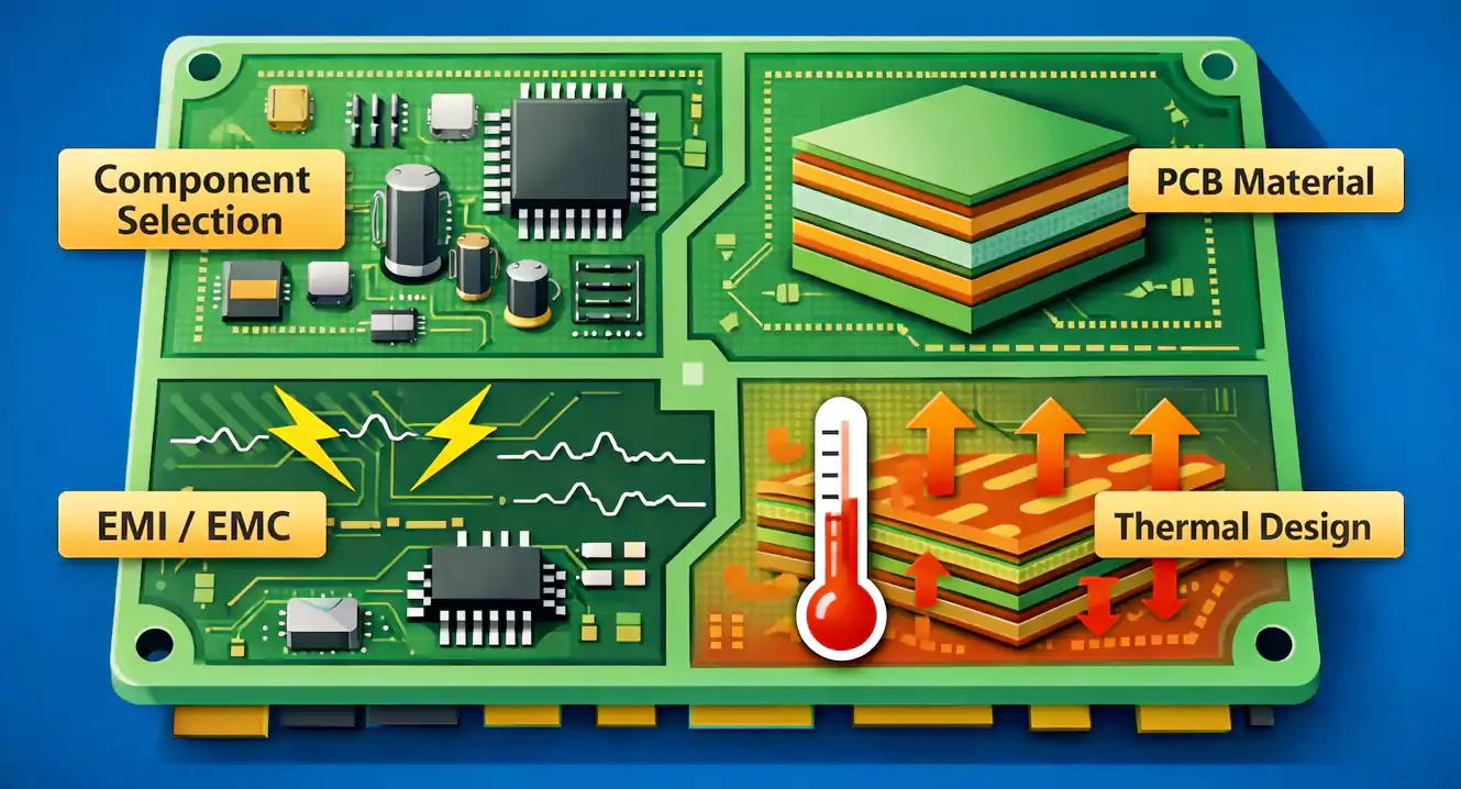
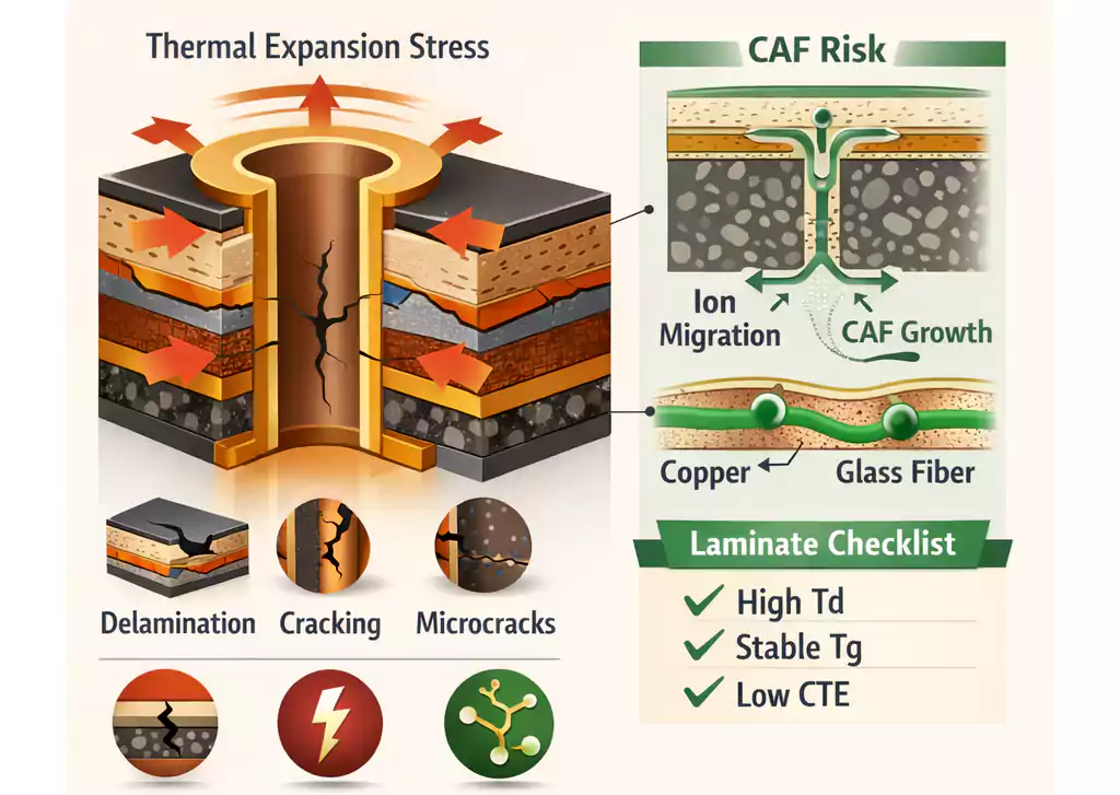
PCB Design Guidelines: choose manufacturable packages (QFP vs BGA), pick the right materials (Tg, CTE, flatness), reduce EMI with smarter grounding and routing, and manage heat for long-term reliability.
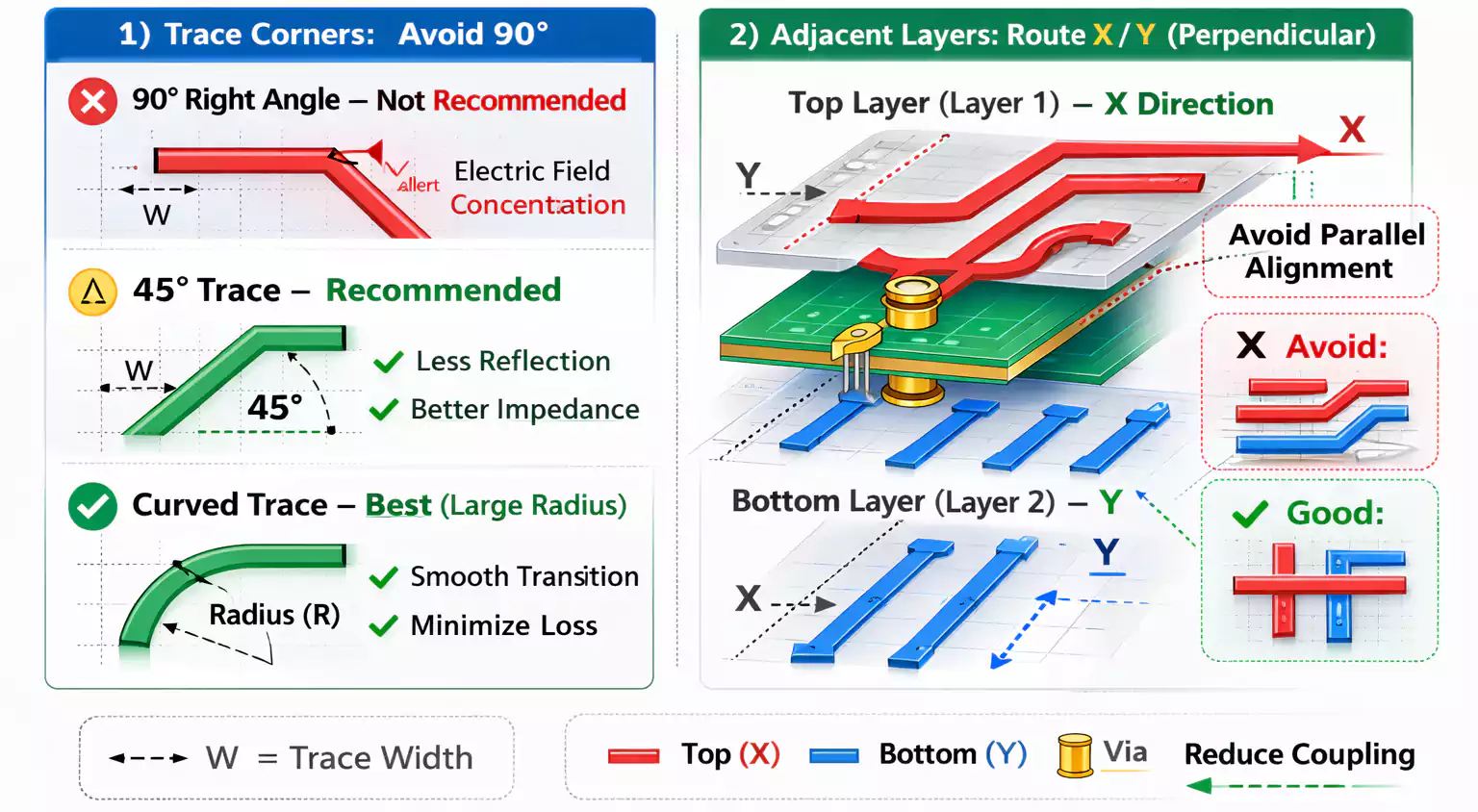
Learn the PCB design rules that reduce EMI, noise, and rework. This guide covers PCB component placement, routing best practices, and trace width/spacing—including analog/digital separation, length matching, thermal relief, edge clearance, and low-impedance power/ground.
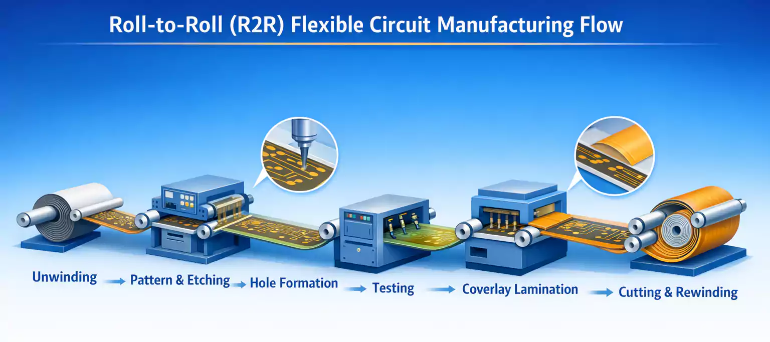
Explore 6 PCB manufacturing methods—stamping/punching, roll-to-roll (R2R), lamination for multilayer boards, subtractive etching, additive copper build-up, and discrete wiring (multiwire). Learn how each works, key pros/cons, and best-fit applications for cost, volume, and reliability.
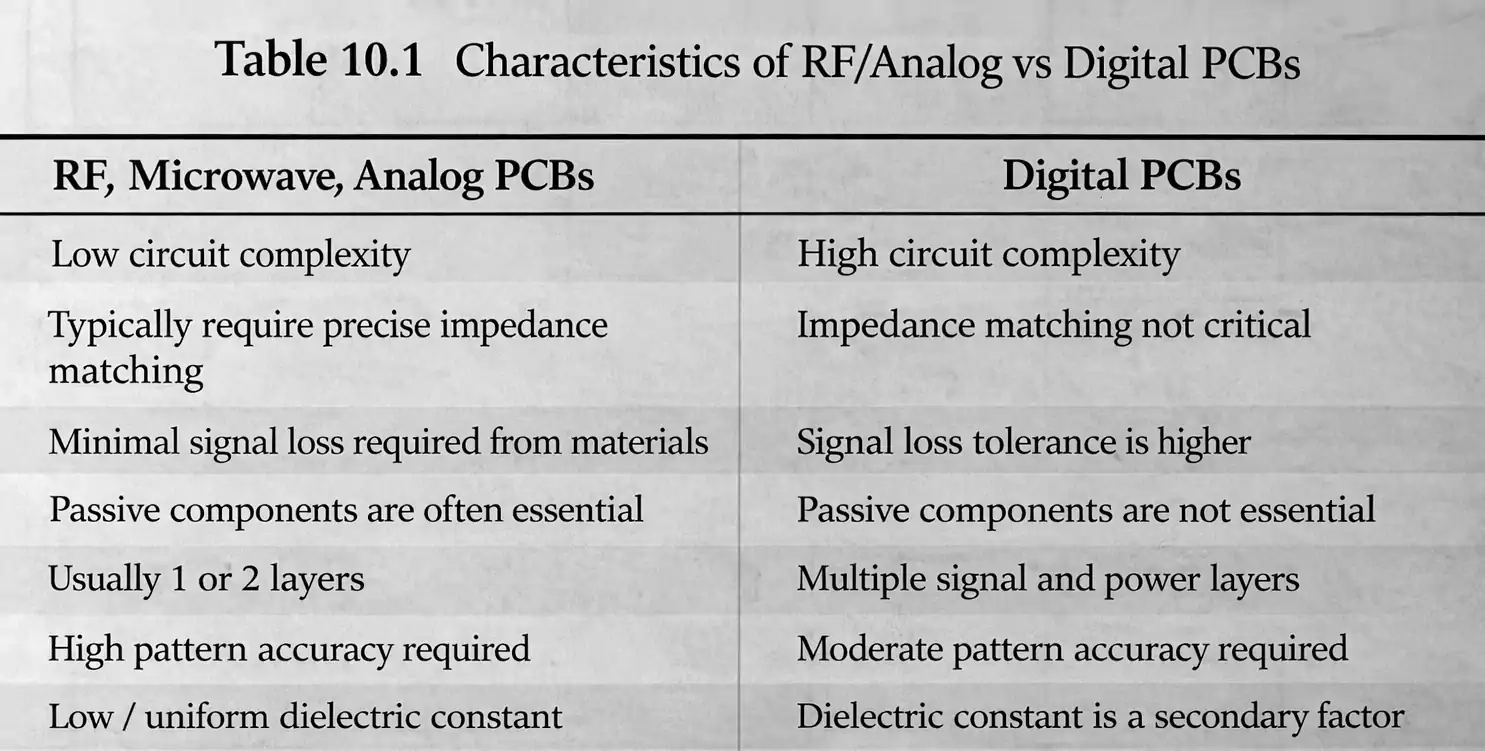
Learn the essentials of RF PCB design—how RF and microwave PCBs differ from digital boards, key layout challenges, and what truly drives high-frequency performance.
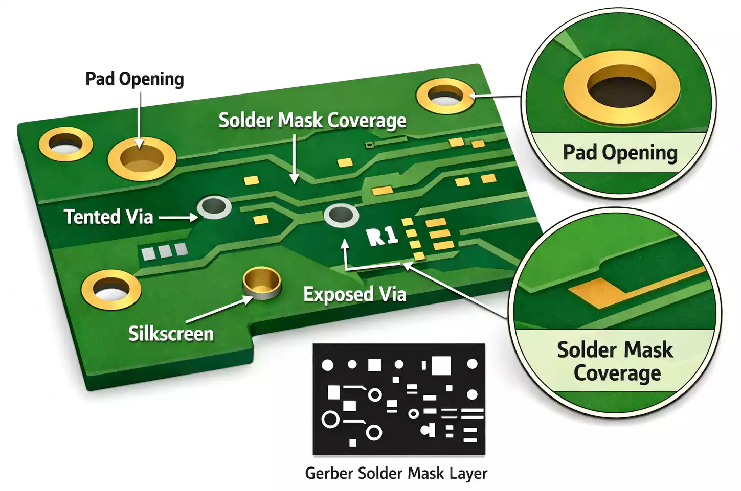
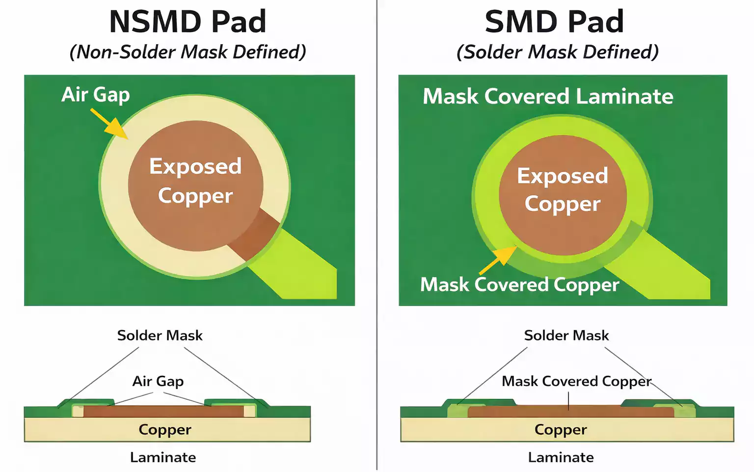
Learn what solder resist (solder mask) is, its types, materials, thickness, and color options. Discover key PCB design rules to prevent solder bridging.
Discover what solder mask is, how it protects PCBs, key design rules, material types, and common issues to avoid for reliable circuit board manufacturing.
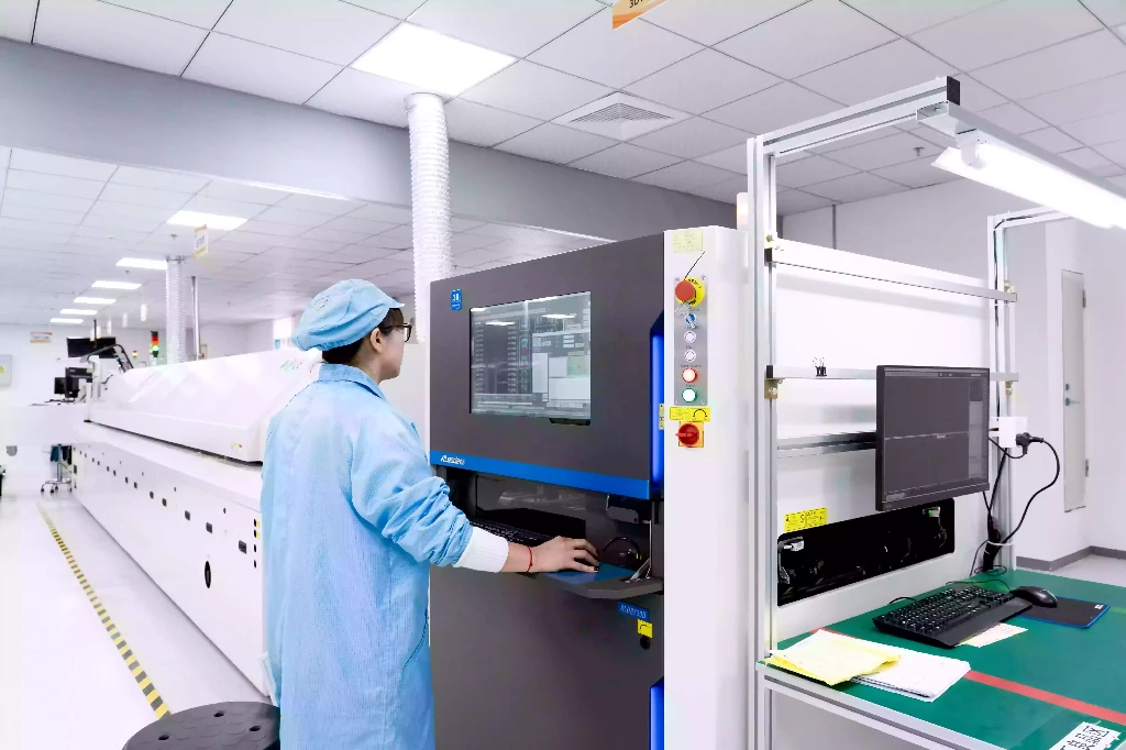
Discover what FQC (Final Quality Control) means in PCB manufacturing and why it’s the last critical step before shipping. Learn the full FQC inspection process, testing methods, and packaging standards that ensure every PCB is defect-free, protected, and ready for reliable performance.