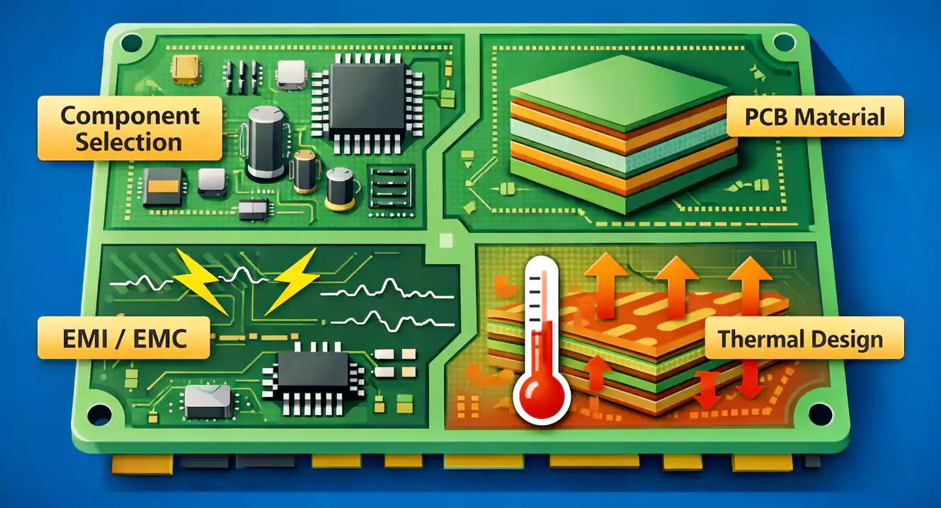
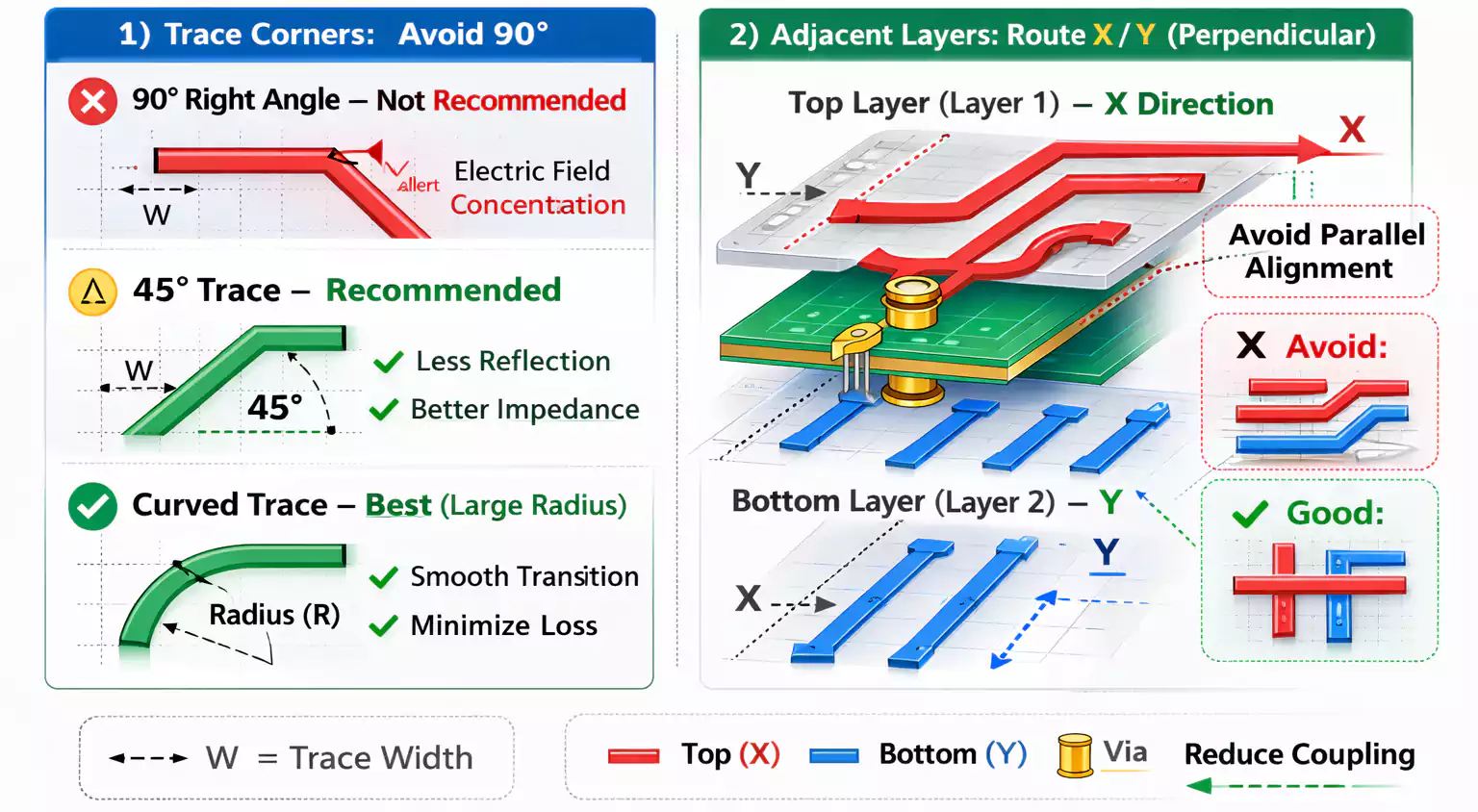
Learn the PCB design rules that reduce EMI, noise, and rework. This guide covers PCB component placement, routing best practices, and trace width/spacing—including analog/digital separation, length matching, thermal relief, edge clearance, and low-impedance power/ground.