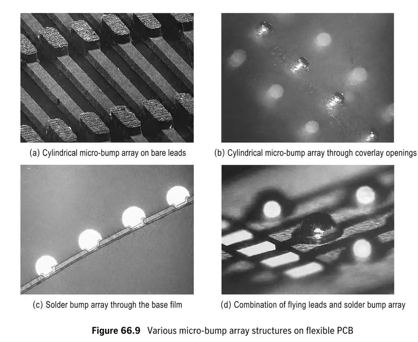
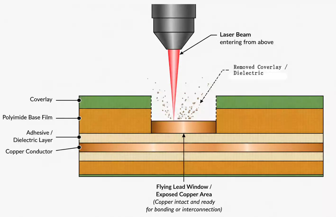
In HDI flex PCB manufacturing, flying lead structures are formed by removing selected dielectric areas and exposing copper conductors for bonding, connection, or assembly.
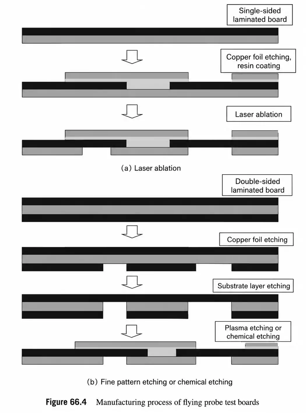
Several processes can be used for this window-opening step, including laser ablation, plasma etching, and chemical etching. For high-volume designs with many openings or large exposed areas, plasma and chemical etching can offer a practical balance of throughput, cost, and material compatibility.
The right HDI flex PCB etching process depends on the window size, polyimide thickness, copper thickness, material type, production volume, and required dimensional control.
Quick Answer
Plasma etching and chemical etching are batch processes used to remove selected dielectric materials in HDI flex PCBs.
Plasma etching works with a wide range of flexible circuit materials but requires vacuum equipment and careful process control.
Chemical etching is especially useful for polyimide etching for flex circuits, including Kapton-type materials, and is well-suited for high-volume or roll-to-roll flex PCB manufacturing.
Compared with laser ablation, plasma and chemical etching are usually more cost-effective when the design has many openings or large window areas.
What Are Plasma Etching and Chemical Etching Used For in Flex PCB Manufacturing?
In flex PCB manufacturing, plasma etching and chemical etching are used to remove selected organic base materials from the circuit. This exposes the copper conductor and creates the required flying lead or windowed lead area.
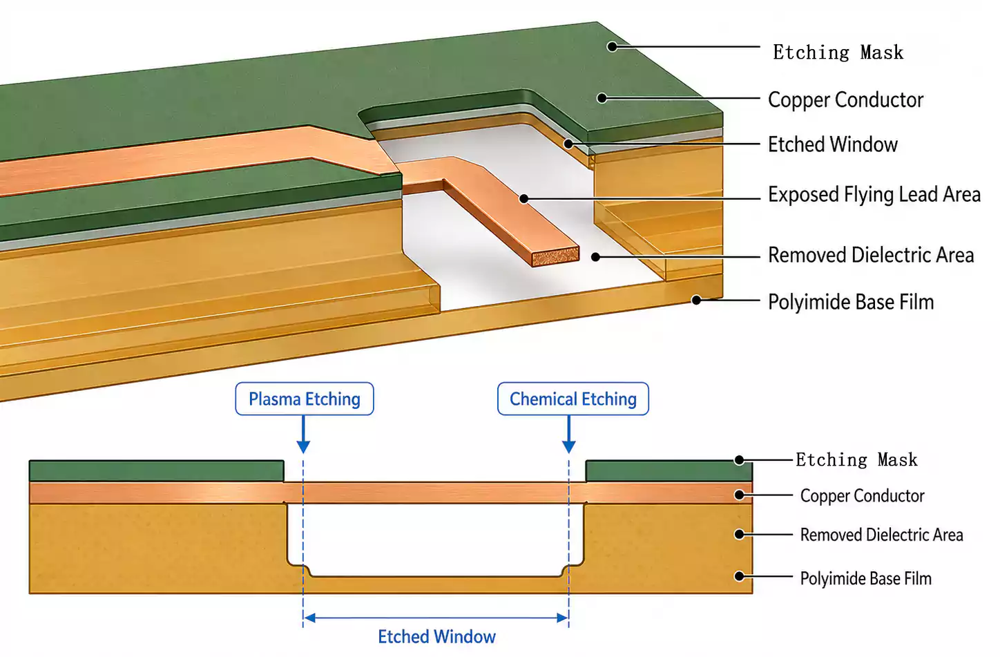
A typical flex PCB window opening process includes:
- Applying a protective mask to copper areas that should not be processed.
- Leaving the window areas exposed.
- Removing the organic dielectric material through plasma or chemical treatment.
- Forming the required openings, holes, or exposed flying lead areas.
The main advantage is that these methods do not process each window individually. Instead, many openings can be processed simultaneously.
This makes plasma etching flex PCB and chemical etching flex PCB processes especially useful for high-density designs with repeated windows or large exposed areas.
Suitable Board Types and Structural Limitations
Both plasma etching and chemical etching can be used for HDI flex PCB flying lead structures, but the actual process choice depends on the board construction.
Single-Sided Flex Circuits
For single-sided flex circuits, both processes are usually easier to apply. The stack-up is simpler, and the areas that need masking or dielectric removal are easier to control.
Double-Sided Flex Circuits
For double-sided flex circuits, the process is more complex.
Plasma and chemical etching are suitable only for certain materials and structures. Double-sided flex circuits may include copper layers, base films, coverlays, adhesives, and plated features that respond differently during etching.
Before selecting either process, engineers should evaluate:
- Material compatibility
- Window size and location
- Masking feasibility
- Copper foil thickness
- Flying lead support
- Risk of over-etching or under-etching
- Whether the stack-up is suitable for batch etching
For this reason, the etching process should be considered early in the design stage, not only after the layout is complete.
Why Plasma and Chemical Etching Work Well for High-Volume Window Opening
The biggest advantage of plasma etching and chemical etching is that they can process multiple holes or windows simultaneously.
This is different from laser ablation.
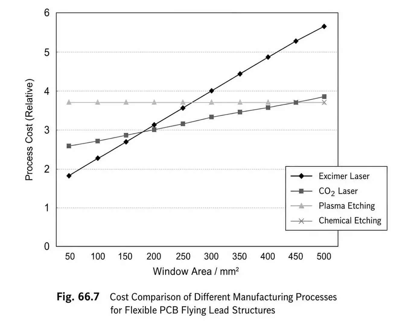
Laser ablation removes material with a focused beam. As the number of windows or total window area increases, processing time also increases. As a result, manufacturing cost usually rises with both window size and window count.
Plasma etching and chemical etching are batch-type processes. Once the masking pattern is prepared, many openings can be processed in the same operation.
These methods are especially cost-effective for:
- Large numbers of repeated openings
- Large-area dielectric removal
- High-density flying lead structures
- High-volume HDI flex PCB production.
- Designs where individual laser processing would be too slow
- Flex circuits suitable for roll-to-roll or horizontal processing
Plasma Etching for HDI Flex PCB Flying Lead Structures
Plasma etching can process almost all types of flexible circuit materials. This broad material compatibility is one of its key advantages.
For materials that are difficult to remove with standard chemical solutions, plasma etching may still be a practical option. However, it also has several important limitations.
Plasma Etching Requires a Vacuum Environment
Plasma etching is typically performed under vacuum. This means the equipment is more complex, and the process environment must be carefully controlled.
For prototyping or low-volume production, the equipment investment may not be economical. For large-scale flying lead production, plasma etching requires significant capital investment.
Batch Accuracy Can Be Difficult to Maintain
When plasma etching is used for batch production under vacuum conditions, it can be difficult to maintain highly consistent etching accuracy across all parts and panel locations.
This may affect:
- Window size consistency
- Edge shape
- Dielectric removal depth
- Exposed copper quality
- Overall production yield
Plasma etching can be effective for volume production, but products with very tight dimensional requirements need strict equipment control and process monitoring.
Plasma Etching Creates a Sloped Window Edge
Depending on the process conditions, plasma etching often creates a window edge with a 30° to 60° slope.
This means the sidewall is not perfectly vertical. Instead, the window edge has a tapered profile.
This may be acceptable for many flying lead designs. However, if the product requires a sharp window boundary, tight spacing, or highly controlled edge geometry, this slope must be considered during the design stage.
Small-Hole Processing Limitations
Plasma etching also has limitations when processing small holes in thicker polyimide materials.
For example, on a 50 μm-thick polyimide substrate, it is difficult to process holes smaller than 100 μm in diameter when the aspect ratio is greater than 0.5:1.
This means plasma etching is useful for batch dielectric removal, but it is not always the best choice for small, high-aspect-ratio openings.
Chemical Etching for Polyimide Flex Circuits
Chemical etching is another low-cost method for high-volume polyimide removal.
Instead of using plasma, this process uses selected chemical solutions to remove polyimide or other organic dielectric materials from exposed areas.
Compared with plasma etching, chemical etching usually requires lower equipment investment. It is also well-suited for continuous production methods, including horizontal roll-to-roll flex PCB manufacturing.
Small-Feature Capability of Chemical Etching
Chemical etching can create relatively small openings in thin polyimide materials.
For example, on a 25 μm-thick polyimide substrate, chemical etching can produce openings smaller than 100 μm in diameter.
This makes chemical etching polyimide processes useful for thin HDI flex circuits, fine-pitch flying lead structures, and high-volume polyimide window opening.
However, chemical etching is highly process-dependent. It requires careful control of:
- Chemical formulation
- Chemical concentration
- Temperature
- Etching time
- Mask adhesion and protection
- Material reaction rate
- Risk of over-etching or under-etching
The process is only reliable when the chemistry, material, and process conditions are well matched.
Polyimide Etching Materials: Kapton and Upilex
Polyimide is one of the most common base materials used in flexible PCBs. However, not all polyimide films respond the same way to chemical etching.
Different polyimide materials have different chemical resistance, thermal stability, and etching behavior.
Kapton Polyimide Etching
For Kapton-type polyimide materials, commonly used etching chemicals include:
- Sodium hydroxide
- Potassium hydroxide
These strong alkaline solutions are often used to remove selected polyimide areas during chemical etching.
Upilex Polyimide Etching
Upilex-type polyimide materials are generally more chemically stable than Kapton materials, which makes them more difficult to etch.
When processing more stable materials such as Upilex-type polyimide, stronger alkaline chemistry is usually required. The process conditions must also be controlled more tightly.
Why Chemical Etching Works Well for Roll-to-Roll Flex PCB Manufacturing
In high-volume production, chemical etching does not require the same level of equipment investment as plasma etching. This makes it suitable for horizontal roll-to-roll, or RTR, manufacturing.
RTR processing is commonly used in the production of continuous flexible circuits. For thin polyimide materials and repeated window structures, chemical etching can provide efficient and cost-effective processing.
Its main advantages include:
- Lower equipment investment
- Good compatibility with continuous production
- High efficiency for large numbers of windows
- Suitability for thin polyimide substrates
- Stable cost even when the number of windows increases
- Good fit for horizontal processing lines
When the material and design are suitable, chemical etching can be one of the most economical methods for producing HDI flex PCB flying lead structures.
Cost Considerations for HDI Flex PCB Etching
Different HDI flex PCB window-opening methods exhibit different cost behaviors.
For plasma etching and chemical etching, the cost is usually less affected by the number or size of openings. These are batch processes, so many windows can be etched in the same operation once the masking pattern is prepared. This makes them more suitable for high-volume production, large-area dielectric removal, or designs with many repeated openings.
Laser ablation works differently. Because the material is removed by a focused beam, processing time increases as the window size or the number of windows increases. For small, high-precision openings, laser ablation can be a good choice. But for large-area or high-count window openings, the cost can rise quickly.
CO₂ laser ablation may also require additional cleaning to remove residue from the window edge or copper surface. However, when the number of openings is high, its faster ablation rate can make it more competitive than slower laser processes.
In general, plasma etching and chemical etching are more cost-effective for batch production, while laser ablation is better suited for smaller, more precise, or lower-volume window-opening requirements.
Process Comparison for HDI Flex PCB Window Opening
| Plasma etching | Works with almost all flex materials; suitable for batch processing | Requires vacuum equipment; high capital investment; batch accuracy can be difficult to control | High-volume window opening where material compatibility is important |
| Chemical etching | Low cost; lower equipment investment; suitable for RTR processing | Highly dependent on chemistry, material type, and process control | High-volume polyimide window opening for thin HDI flex circuits |
| Excimer laser ablation | High precision; suitable for fine features | Slow processing speed; high cost when many windows are required | Small, high-precision, low-count openings |
| CO₂ laser ablation | Faster ablation rate; more competitive when opening count is high | Lower edge quality and dimensional accuracy; may require post-cleaning | Larger openings or higher window counts where extreme precision is not required |
How to Choose the Right HDI Flex PCB Etching Process
The best process depends on the design, material, production volume, and cost target.
- Use Laser Ablation When Precision Is the Priority
- Use Plasma or Chemical Etching for High-Volume Production
- Use Plasma Etching When Material Compatibility Is Critical
- Use Chemical Etching When the Material Is Suitable
- Pay Attention to the Polyimide Type
FAQ: Plasma Etching and Chemical Etching for HDI Flex PCB
What is plasma etching in flex PCB manufacturing?
Plasma etching in flex PCB manufacturing is a batch process used to remove selected organic dielectric material from a flexible circuit. It can expose copper conductors and create window areas for flying lead structures.
What is chemical etching in HDI flex PCB manufacturing?
Chemical etching uses controlled chemical solutions to remove selected dielectric materials, especially polyimide. It is commonly used for high-volume polyimide window opening in flexible circuits.
Plasma etching vs chemical etching: which is better for HDI flex PCB?
Plasma etching offers wider material compatibility, but it requires vacuum equipment and higher capital investment. Chemical etching is usually more cost-effective for suitable polyimide materials and high-volume production.
Is chemical etching suitable for polyimide flex circuits?
Yes. Chemical etching is often used for polyimide etching in flex circuits. However, the chemical solution and process parameters must match the specific polyimide material, such as Kapton-type or Upilex-type films.
When is laser ablation better than plasma or chemical etching?
Laser ablation is usually better for small, high-precision, low-count openings. Plasma etching and chemical etching are often more economical when the design requires many openings or large-area dielectric removal.
Conclusion
Plasma etching and chemical etching are practical HDI flex PCB etching methods for flying lead structures, especially when the design requires many openings or large-area dielectric removal.
Plasma etching offers broad material compatibility, while chemical etching can provide a lower-cost solution for suitable polyimide materials and roll-to-roll production. The best choice depends on window size, material type, copper thickness, production volume, and dimensional requirements.
For high-volume flying lead flex PCB manufacturing, the right etching process can improve efficiency, control cost, and support reliable conductor exposure. FastTurnPCB supports customers in evaluating suitable flex PCB manufacturing processes based on design, material, and production needs.