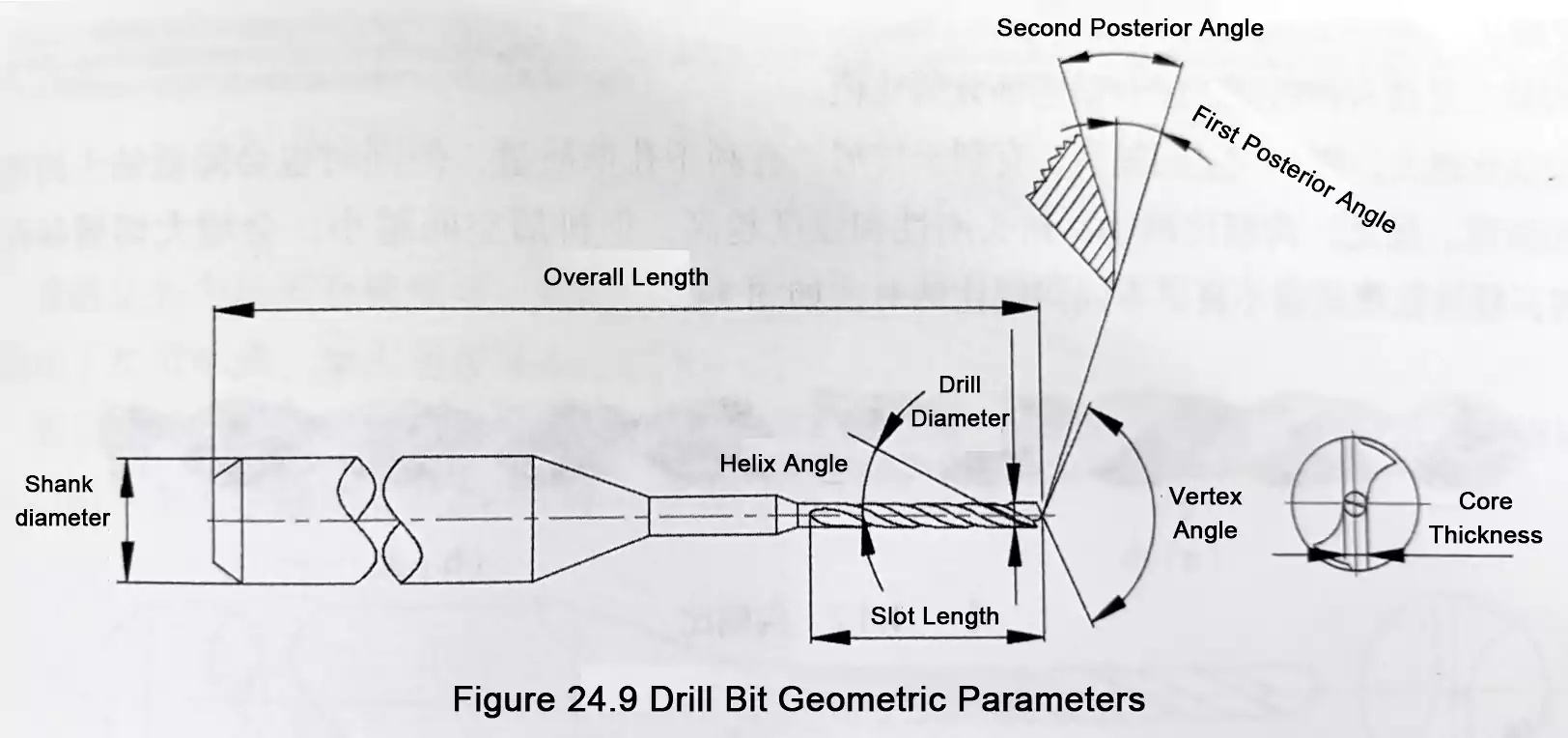
PCB fabrication low cost guide: smart choices on materials, thickness, finish, testing & lead time, plus 2026 supplier rankings—affordable boards without risk.
Learn how to choose PCB dielectric stackup—single vs. multi prepreg—using pressed thickness, resin content, and glass style to control impedance, cost, and manufacturability.
Add QR Code PCB to your production with practical tips on laser marking, silkscreen, size, placement, and traceability to ensure reliable scanning and serial tracking.
Create a production-ready pcb schematic — from symbols and netlists to Gerber export and PCBA handoff. Follow a clear step-by-step checklist and grab downloadable templates.
PCB Trace Guide: Learn how to size trace width for current and temperature, control impedance for high-speed signals, and validate designs with trace width calculators.
Surface mount PCB guide: design tips, stencil & solder paste advice, reflow best practices, inspection and troubleshooting to move prototypes into production.
Learn how copper foil roughness drives GHz signal loss in high-speed PCBs. Clear skin-effect primer, Df test highlights, and practical fixes—use low-profile or RTF foils to cut insertion loss.
Quick guide to choosing copper foil for high-density PCBs: HTE, low-roughness, RTF and resin-specific foils to boost reliability, yield, and high-speed signals.
Discover 3 HDI strategies—fine-line etching, extra layers, and microvias—to increase PCB wiring density while maintaining yield and high-frequency performance.
Dielectric constant and permittivity: Learn Dk vs Df, why FR-4 and Teflon differ, and how to pick low-loss PCB materials for reliable high-speed designs.