In high-density flexible circuits, a Flex PCB micro bump array provides a compact three-dimensional interconnect structure for fine-pitch assembly. Instead of relying solely on flat pads, microbumps create raised contact points that support chip bonding, package interconnection, test probing, and other advanced termination requirements.
These structures are commonly used in HDI flex PCBs, flip-chip assembly, CSP interconnection, and precision probe applications. By controlling bump shape, material, pitch, and fabrication method, designers can improve connection density, contact reliability, and assembly flexibility in compact electronic products.
This article explains the common shapes, materials, applications, and manufacturing methods of micro bump arrays on flexible PCBs.
What Is a Flex PCB Micro Bump Array?
A Flex PCB micro bump array is a group of small raised structures selectively formed on specific areas of a flexible circuit. These bumps are usually built on conductor pads, exposed copper areas, window openings, or flying lead structures.
Functionally, they are similar to BGA solder balls on rigid PCBs. However, because flexible PCBs are thin, bendable, and mechanically sensitive, the bump material, shape, window design, and fabrication process must be carefully controlled.
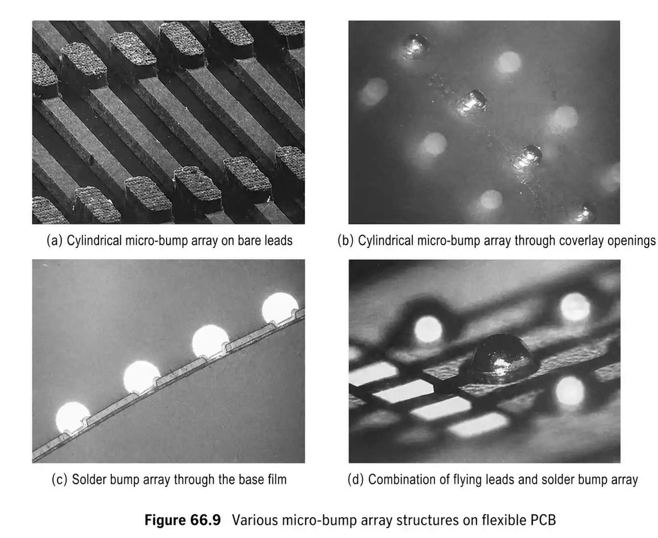
Micro bumps are not simply “small solder balls.” Depending on the process, they can be spherical, flat-topped, dome-shaped, column-like, disk-like, or formed through a dielectric layer.
Why Use Flexible PCBs with Micro Bump Arrays
Micro bump arrays are mainly used when a flexible circuit needs a compact, high-density, or specialized connection interface.
In many miniaturized electronic products, the number of interconnect points continues to increase while available space shrinks. A flat pad only provides a two-dimensional contact surface. For some chip packages, probe structures, and micro-interconnect designs, a raised bump structure provides a more stable and practical contact point.
Key benefits include:
- Higher interconnect density
- More reliable contact geometry
- Better suitability for flip-chip and CSP assembly
- Improved contact performance for test probes
- Compatibility with flying lead and double-sided access structures
For HDI flex PCB termination, microbump arrays can help address connection challenges that are difficult to address with standard flat pads alone.
Where Micro Bump Arrays Can Be Formed
Micro bump arrays are not limited to standard pad areas. Depending on the product design and process flow, they can be formed on several types of flex PCB structures.
| Flex circuits with flexible solder mask | Selected openings are created to expose pad areas, and micro bumps are formed in those openings. |
| Exposed conductor surfaces | A plating mask defines the bump locations directly on exposed copper or conductor areas. |
| Flying lead structures without solder mask | Micro bumps can be formed on delicate flying lead structures for special interconnection needs. |
| Through-dielectric structures | Bumps can be built through the dielectric layer to provide access from the opposite side of the flex circuit. |
Flex Circuits with Flexible Solder Mask
On flexible circuits with a photosensitive solder mask, selected openings can be created to expose the required pad areas. Micro bumps can then be formed in these openings.
This method is similar in concept to the formation of BGA structures on rigid PCBs, but it must account for the circuit's flexibility and thinner construction.
Exposed Conductor Surfaces
Micro bump arrays can also be formed directly on exposed conductor layers. In this case, a plating mask defines the locations of the bumps.
This approach is especially useful when smaller bumps, tighter pitch, or more controlled bump shapes are required.
Flying Lead Structures Without Solder Mask
Many microbump arrays are also built on flying-lead structures without solder mask coverage.
In a flying lead structure, the conductor is locally exposed and may not have full dielectric support. This makes the structure more delicate, but it also allows special interconnection methods.
With proper design, stable micro bumps can be formed through the dielectric layer on the opposite side of the flex circuit, creating a reliable bump array for advanced connection needs.
This type of structure is useful when the design requires thin construction, two-sided access, or a highly compact termination area.
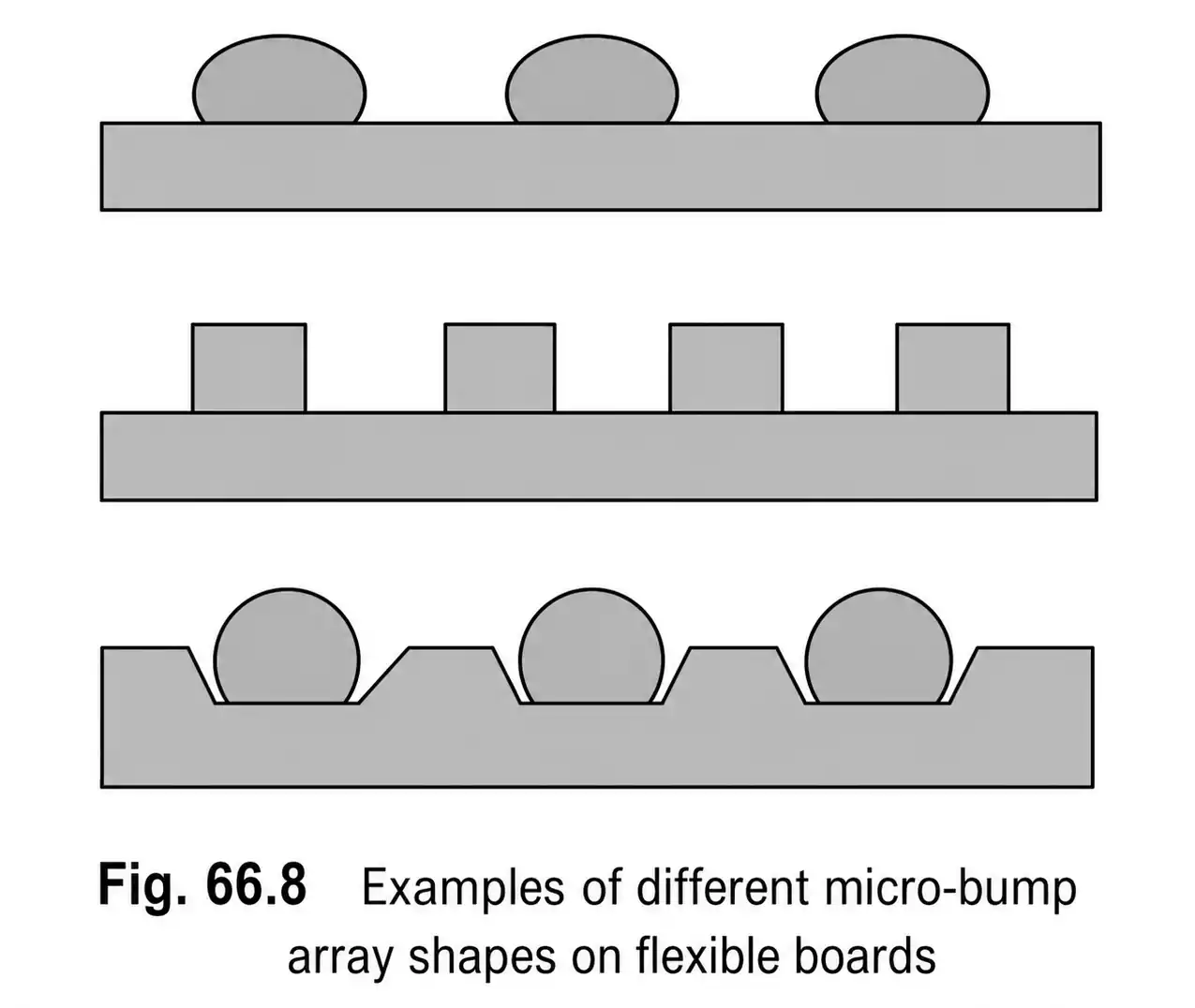
Common Micro Bump Shapes on Flexible PCBs
Microbumps on flexible PCBs can be formed in many shapes. The final geometry depends on the material system, window opening, plating process, and reflow process.
Common micro bump shapes include:
- Spherical bumps
- Flat-top bumps
- Dome-shaped bumps
- Rectangular or column-like bumps
- Flat disk-like bumps
- Bumps formed through the full dielectric thickness
Spherical bumps are closer to conventional solder ball structures and are commonly used for solder-based interconnection. Flat-top or column-like bumps are often better suited for probe contact, compression contact, or applications where consistent bump height is important.
How Different Micro Bump Shapes Are Formed
The shape of a micro bump is strongly influenced by the manufacturing method.
| Solder paste + reflow | Spherical bump | Larger solder bumps and solder-based interconnection |
| Electroplating | Flat-top, dome-shaped, column-like, or composite bump | Fine-pitch, small-size, and non-spherical bump structures |
| Combined metal plating | Customized bump profiles | Applications requiring specific hardness, height, or contact performance |
Reflowed Solder Bumps on Flexible Circuits
Spherical bumps are commonly formed with a solder reflow process.
Solder paste can be dispensed or screen printed onto the pad area. During reflow, the solder melts, and surface tension pulls it into a rounded shape. This makes it relatively easy to create solder bumps on flexible circuits.
This process is suitable for relatively large solder bumps, but it has limited ability to form precise non-spherical structures.
Electroplated Micro Bumps
Electroplating can be used to create smaller bumps and more complex bump shapes.
Copper, nickel, gold, tin, and combined plating systems can be used to produce flat-top, dome-shaped, column-like, or other customized bump profiles. By adjusting the metal combination, plating thickness, and process sequence, manufacturers can control both the shape and performance of the bump.
Electroplated micro bumps are especially useful for fine-pitch micro bump arrays and non-spherical bump structures.
Common Materials Used for Flex PCB Micro Bumps
The material selection depends on the final assembly method and contact requirements.
Common materials include:
- Tin or tin-based solder
- Copper
- Nickel
- Gold
- Copper/nickel/gold combinations
- Other composite plated metal structures
Tin-based bumps are commonly used for soldering applications. Copper, nickel, gold, and multilayer metal combinations are often used when the bump must provide harder contact, better wear resistance, or more stable electrical performance.
Changing the metal ratio or plating stack can directly affect bump height, shape, hardness, conductivity, solderability, and contact reliability.
Fine Pitch Micro Bump Array Capability
With an optimized process, a fine-pitch microbump array can be formed on very thin, flexible circuit materials.
For example, on a dielectric layer about 50 μm thick, it is possible to create micro bump arrays with a pitch of about 100–150 μm.
This makes micro bump arrays highly suitable for HDI flex circuits, but it also means the process requires tight control of:
- Window size
- Plating thickness
- Dielectric thickness
- Registration accuracy
- Bump height uniformity
Typical Applications of Micro Bump Arrays on Flexible PCBs
Most micro bump arrays on flexible PCBs are designed to support terminal assembly in HDI flex circuits.
| Flip-chip assembly | Provides a fine-pitch connection interface between the chip and flex circuit |
| CSP interconnection | Supports compact package-to-board transition |
| Test probe contact | Creates raised and repeatable contact points |
| HDI flex PCB termination | Enables high-density termination in compact electronic modules |
Flip-Chip Assembly
In flip-chip assembly, the chip must connect directly to the circuit substrate. A micro bump array provides a fine-pitch, high-density connection interface between the chip and the flex circuit.
CSP Interconnection
Chip-scale packages require very compact and precise interconnect structures. Microbump arrays can serve as a high-density interface between the package and the flexible circuit.
Test Probe Contact
For test fixtures and probe arrays, micro bumps provide raised, repeatable contact points. Flat-top and column-like bumps are especially useful when the application requires stable mechanical contact.
HDI Flex PCB Termination
Micro bump arrays can also be used as high-density termination structures in compact electronic modules, display assemblies, sensors, medical electronics, and fine-pitch connector systems.
Flex PCB Micro Bump Manufacturing Methods
Flex PCB micro bump arrays are generally produced using two main process routes.
Method 1: Solder Paste Dispensing or Screen Printing Followed by Reflow
This method is similar to the process used for BGA solder ball formation on rigid PCBs.
The basic process is:
- Open the pad area or expose the connection surface.
- Apply solder paste by liquid dispensing or screen printing.
- Reflow the solder paste.
- Allow surface tension to form a spherical bump.
- Cool the structure to create a solid solder bump.
This process is mature and practical for relatively large solder bumps. However, because molten solder naturally tends to form a rounded shape, this method is not ideal for very small pitch arrays or non-spherical bump designs.
Method 2: Electroplating for Small or Non-Spherical Micro Bumps
Electroplating is used when the design requires smaller bumps, tighter pitch, or more controlled bump geometry.
The basic process is:
- Apply a plating mask on the flex circuit surface.
- Open the areas where bumps will be formed.
- Electroplate tin, copper, nickel, gold, or a metal combination.
- Control the bump height, profile, and material stack.
- Remove the mask to reveal the finished micro-bump array.
Electroplating offers better control over bump height and shape. It can be used to make flat-top, column-like, dome-shaped, or composite metal bump structures.
By combining different plating processes, manufacturers can create a wide variety of microbump designs to meet diverse assembly and contact requirements.
Key Factors That Affect Micro Bump Shape and Size
The final shape of a micro bump is controlled by several design and process variables.
| Dielectric thickness | Affects opening depth, bump height, and structural support |
| Window opening size | Controls lateral spread and bump width |
| Opening aspect ratio | Influences whether the bump becomes spherical or disk-like |
| Plating mask design | Helps control sidewall shape, height, and bump boundary |
| Metal stack and plating ratio | Affects hardness, conductivity, shape, and contact reliability |
Dielectric Thickness
Dielectric thickness affects the opening depth, bump height, structural support, and plating profile.
A thicker dielectric may require a deeper opening and can influence how the bump connects to the conductor layer.
Window Opening Size
The opening size controls the bump's lateral spread.
A larger opening usually allows the bump to spread wider and become flatter. A smaller opening restricts deposition and may result in a more spherical or columnar shape.
Opening Aspect Ratio
The aspect ratio of the window opening has a major effect on bump geometry.
When the aspect ratio is high, the resulting bump tends to be closer to a spherical shape. When the aspect ratio is low, the bump tends to become a flatter, disk-like structure.
Plating Mask Design
A well-designed plating mask helps form bumps with straight sidewalls, controlled height, and clear boundaries.
Poor mask design can lead to inconsistent bump height, unstable edge definition, and reduced array reliability.
Metal Stack and Plating Ratio
Different metals have different plating behavior, hardness, wetting characteristics, and surface profiles.
Adjusting the combination and ratio of copper, nickel, gold, tin, or other metals can significantly change the final bump shape and performance.
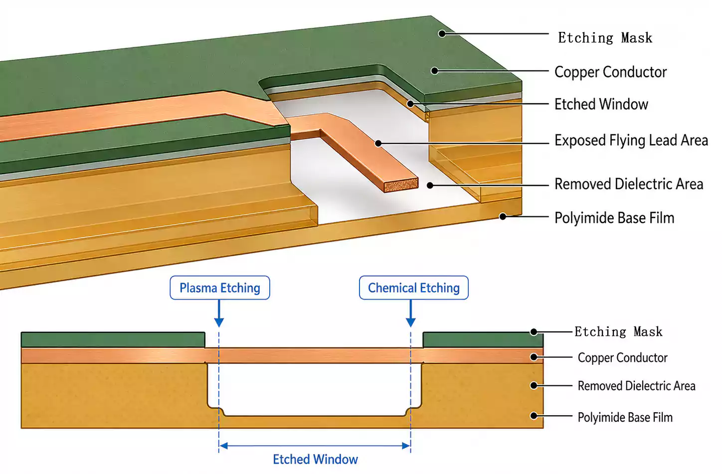
Window Opening Processes for Micro Bump Arrays
Window formation is a critical step in micro bump array manufacturing. The bump often needs to be built through or inside openings in the dielectric layer, coverlay, or solder mask.
Common window opening methods include:
- Mechanical drilling
- Laser drilling
- Plasma etching
- Chemical etching
Mechanical Drilling
Mechanical drilling can be used when the micro bump structure needs to pass through the entire dielectric layer.
This method can support through-dielectric bump structures, but hole quality, registration, and dimensional control are important.
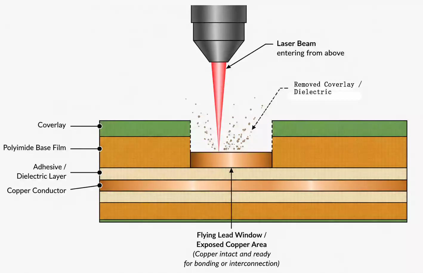
Laser Drilling
Laser drilling can create high-precision openings for fine-pitch micro bump arrays.
It is well-suited for small windows, tight registration, and HDI flex PCB structures that require accurate dielectric removal.
Plasma Etching and Chemical Etching
When large-volume, lower-cost window formation is required, plasma etching or chemical etching may be used.
These methods are useful for batch processing, but the best choice depends on the dielectric material, window size, edge quality, production volume, and cost target.
FAQ About Flex PCB Micro Bump Arrays
What is a Flex PCB micro bump array?
A Flex PCB micro bump array is a group of small raised conductive structures formed on a flexible circuit to support high-density interconnection, chip bonding, package assembly, or test contact.
What are micro bumps used for in flexible PCBs?
Micro bumps are commonly used for flip-chip assembly, CSP interconnection, test probe contact, and HDI flex PCB termination.
What materials are used for flexible PCB micro bumps?
Common materials include tin-based solder, copper, nickel, gold, and copper/nickel/gold plated combinations.
How are micro bumps made on flexible circuits?
They are usually made by dispensing solder paste and then reflowing, or by electroplating through a defined plating mask.
What affects the shape of a micro bump?
The shape is affected by dielectric thickness, window opening size, opening aspect ratio, plating mask design, metal stack, and plating process conditions.
Conclusion
A Flex PCB micro bump array is more than a raised pad structure. It is a controlled interconnect solution for fine-pitch assembly, HDI flex PCB termination, flip-chip bonding, CSP interconnection, and probe contact.
Its performance depends on the right combination of bump shape, material, dielectric thickness, window design, plating mask, and manufacturing process. Spherical, flat-top, dome-shaped, column-like, and disk-like bumps each serve different assembly needs.
For advanced flexible circuits, micro bump arrays should be designed in conjunction with the final package, contact method, pitch requirements, and reliability target. When properly engineered, they help improve connection density, assembly accuracy, and long-term interconnect reliability.