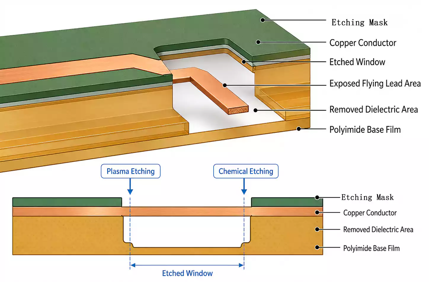
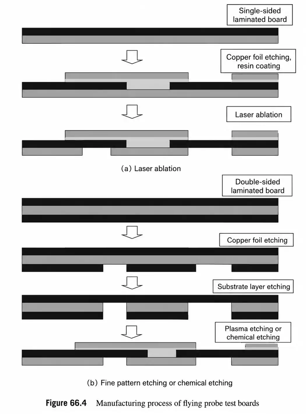
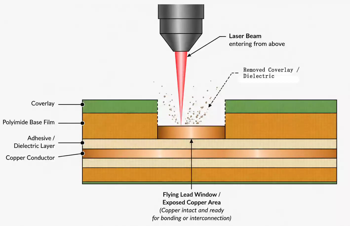
Flex PCB laser ablation is an industrial material removal process used to create precise openings in flexible circuit materials. In HDI flexible PCBs, it is often used to expose selected copper conductors for flying lead structures, bonding areas, or fine-pitch interconnection.
For flying lead window openings, laser ablation removes selected coverlay, base film, or dielectric material while keeping the copper conductor intact as much as possible. This is important because the exposed copper lead has limited mechanical support after the surrounding material is removed.
Different laser technologies, including excimer, UV YAG, and CO2 lasers, can be used for this process. Each method offers a different balance of accuracy, processing speed, edge quality, thermal impact, and cost.
This article explains how laser ablation is used in HDI flex PCB manufacturing and how to choose the right process for flying lead window opening.
Quick Answer
For HDI flex PCB laser ablation, the best process depends on window size, accuracy requirements, copper thickness, production volume, and cost target.
- Excimer laser ablation is best for high-precision small windows below 50 μm, but it is slow and costly for large quantities.
- UV YAG laser ablation offers higher efficiency and good processing quality, but becomes less practical when the window area exceeds about 10,000 μm².
- CO2 laser ablation can be efficient for window widths above 70 μm, but it results in lower edge quality, lower dimensional accuracy, and greater thermal impact.
- For fine flying lead structures, especially window widths below 100 μm with 18 μm copper, CO2 laser energy must be carefully controlled.
Why Window Opening Matters in Flying Lead Flex PCBs
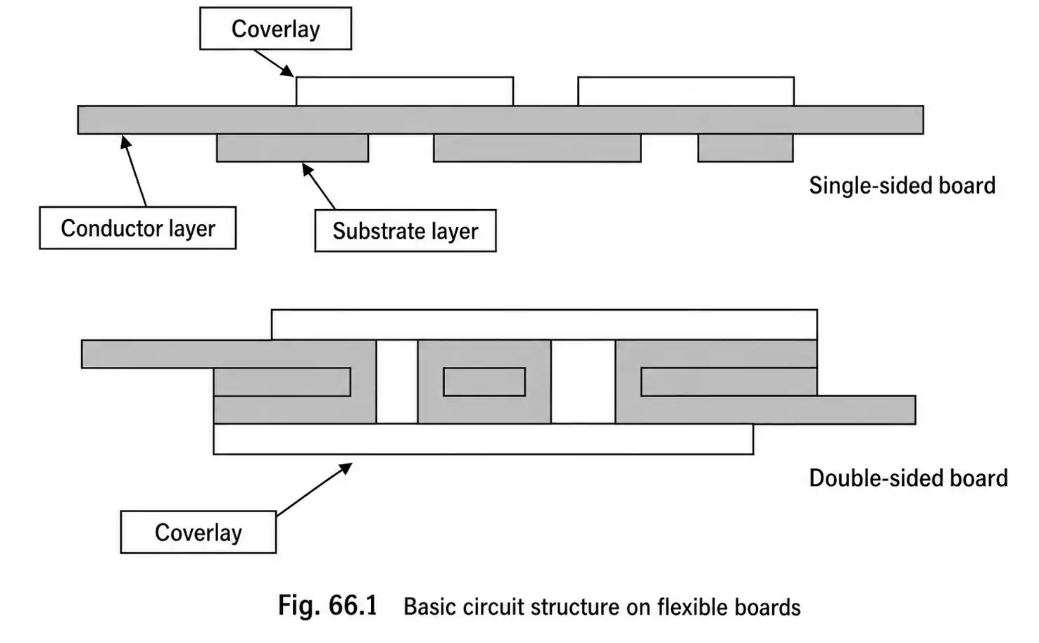
In a flying lead flex PCB, a window opening removes selected coverlay, base film, or dielectric material to expose the copper conductor. This exposed copper area is then used for bonding, soldering, or fine-pitch electrical connections.
Because the copper lead has limited support after material removal, the process must control edge quality, dimensional accuracy, cleanliness, and thermal impact. Poor window opening can cause copper damage, edge defects, residue, or reduced connection reliability.
The goal is to create a clean, accurate opening without damaging the exposed copper conductor. For reliable results, the laser ablation process should be matched to the window size, material stackup, copper thickness, and production requirements.
Main Laser Ablation Methods for HDI Flex PCB Window Opening
Several laser technologies can be used for flying lead window opening. The most common options include excimer laser, UV YAG laser, TEA CO2 laser, and diamond CO2 laser.
| Excimer laser | Very high precision | Slow processing speed | Small, fine windows |
| UV YAG laser | Good balance of quality and efficiency | Efficiency drops for larger windows | Small to medium window areas |
| TEA CO2 laser | High throughput for wider windows | Lower edge quality and accuracy | Wider openings |
| Diamond CO2 laser | High productivity in suitable ranges | Higher thermal impact | Larger window openings |
Excimer Laser Ablation for Flex PCB
Best for high-precision small windows
Excimer laser ablation for flex PCB is well-suited for small window openings in HDI flexible circuits. It provides very high processing accuracy and can create minimum processing widths below 50 μm.
This makes it a strong choice for fine-flying lead structures that require tight dimensional control and clean feature definition.
Material compatibility
Another key advantage of excimer laser processing is broad material compatibility. It can process almost all types of flexible circuit materials, which is useful for complex HDI flex PCB stackups.
Residue control
During excimer laser ablation, carbon residue may appear near the window edge. In most cases, this residue can be removed by wet cleaning to maintain a clean opening area.
Key advantages
- Suitable for small window openings
- Minimum processing width below 50 μm
- High-dimensional accuracy
- Compatible with many flexible PCB materials
- Low risk of damage to flying lead structures
- Good edge definition for fine features
Main limitation
The biggest drawback of excimer laser ablation is speed. The process is relatively slow. When a board requires many windows, processing time and cost increase significantly.
Best-fit applications
Excimer laser ablation is most suitable for:
- High-precision HDI flex PCBs
- Fine flying lead structures
- Small window openings
- Complex flex material systems
- Designs where accuracy is more important than throughput
UV Laser Ablation for HDI Flex PCB
Higher efficiency than excimer laser processing
Compared with excimer laser ablation, UV laser ablation for flex PCB provides much higher production efficiency. YAG-type UV laser ablation can cut both flexible base material and copper foil with good processing quality.
This makes UV YAG laser ablation suitable for larger processing areas in HDI flexible PCB manufacturing.
Good balance between quality and throughput
UV laser processing has a relatively small heat-affected zone. This helps reduce the risk of damage to the flying lead structure during fabrication.
For many HDI flex PCB designs, UV YAG laser ablation offers a practical balance between precision, quality, and speed.
Size limitation
UV laser ablation is not always efficient for very large windows. As the window size increases, processing efficiency drops noticeably.
In practical production, when the window area exceeds about 10,000 μm², UV laser ablation becomes less practical.
Key advantages
- Higher efficiency than excimer laser ablation
- Good cutting quality for base materials
- Can process conductor copper foil
- Suitable for wider HDI flex PCB window opening areas
- Reduced risk of flying lead damage
- Good overall process quality
Main limitation
The efficiency of UV laser ablation decreases as the window size increases. For very large windows, it may no longer be the most practical or cost-effective process.
Best-fit applications
UV YAG laser ablation is most suitable for:
- Small to medium window openings
- HDI flex PCBs require both quality and efficiency
- Applications involving base material and copper foil processing
- Designs where excimer laser processing is too slow
- Flying lead structures that require controlled thermal impact
CO2 Laser Ablation for Flex PCB
Higher throughput for wider windows
CO2 laser ablation for flex PCB can also be used for HDI flying lead window opening. TEA CO2 lasers and diamond CO2 lasers can provide relatively high production efficiency when the window width is greater than 70 μm.
For applications where throughput is a major concern, CO2 laser ablation may offer a practical advantage.
Lower edge quality and dimensional accuracy
Compared with excimer and UV lasers, CO2 laser ablation generally produces lower edge quality and lower dimensional accuracy.
This means CO2 laser processing is less suitable for very fine windows or designs that require strict edge definition.
Residue and cleaning requirements
After CO2 laser ablation, residue may remain on the copper foil surface. To keep the board surface clean, plasma etching is often used after laser processing to remove these residues.
Local masking for better results
Using a local mask on the copper foil surface can improve the quality and speed of CO2 laser ablation. The mask protects areas that should not be ablated and helps reduce unwanted laser impact on the surrounding copper surface.
Key advantages
- High efficiency when the window width is above 70 μm
- Suitable for some larger window openings
- Faster material removal than excimer laser processing
- Potential cost advantages in suitable production conditions
Main limitations
- Lower window edge quality
- Lower dimensional accuracy
- More residue on copper surfaces
- Greater thermal impact
- Requires careful energy control
- May require plasma cleaning after ablation
Best-fit applications
CO2 laser ablation is most suitable for:
- Window widths above 70 μm
- Larger window openings
- Applications where production speed is important
- Designs with less demanding edge-quality requirements
- Processes that can include masking and post-cleaning steps
Thermal Impact on Flying Lead Structures
Flying lead structures are sensitive because the copper conductor is partially exposed and has limited support from the surrounding dielectric material.
Laser energy, heat input, and material removal behavior can directly affect reliability.
Excimer and UV laser processes
Excimer and UV laser ablation can reduce the risk of damage to the flying lead structure. These processes are better suited for fine features, high-density routing, and small window openings.
CO2 laser process
CO2 laser processing generates more heat during ablation. Therefore, energy control is especially important when processing fine flying lead structures.
Extra care is needed when:
- The window width is below 100 μm
- The copper foil thickness is about 18 μm
- The flying lead is narrow or delicate.
- The surrounding material is sensitive to heat.
- The product requires strict edge quality and dimensional accuracy.
If CO2 laser energy is too high, the exposed copper may suffer from heat damage, deformation, edge defects, or reduced bonding reliability.
Laser Ablation Process Comparison
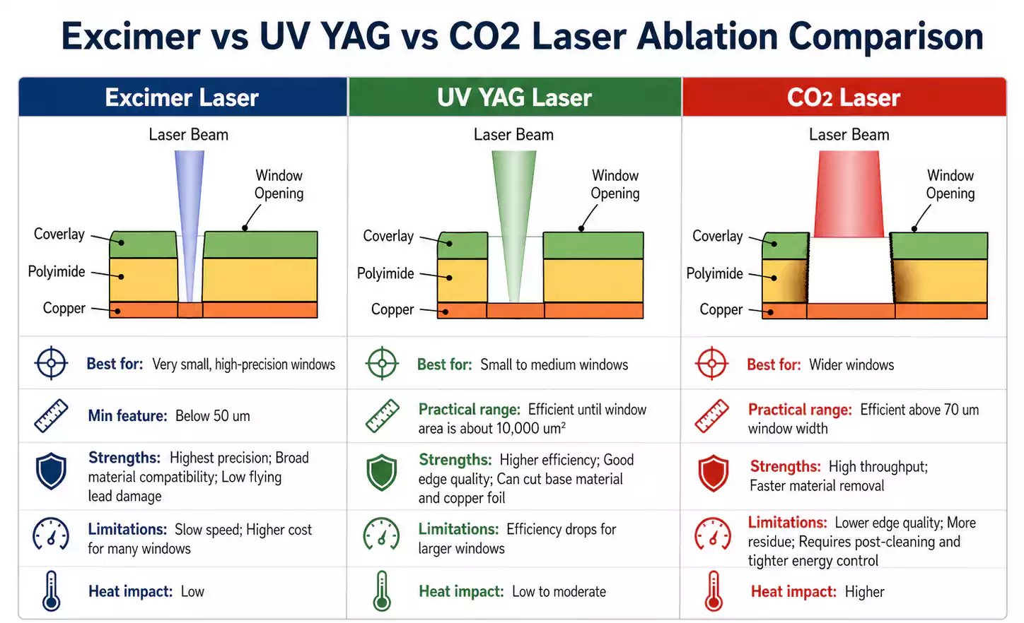
| Excimer laser ablation | Below 50 μm processing width | Highest precision, broad material compatibility, low flying lead damage | Slow speed, high cost for many windows | Fine, high-precision small windows |
| UV YAG laser ablation | Practical for small to medium windows | Higher efficiency, good quality, can cut base material and copper foil | Less practical above 10,000 μm² window area | Balanced quality and throughput |
| TEA CO2 laser ablation | Efficient above 70 μm window width | High productivity for wider openings | Lower edge quality, lower accuracy, higher thermal impact | Wider windows with throughput priority |
| Diamond CO2 laser ablation | Efficient above 70 μm window width | Good production efficiency in suitable ranges | Similar CO2 limitations: heat, residue, accuracy control | Larger openings with post-cleaning support |
How to Choose the Right Flex PCB Laser Ablation Process
The right flex PCB laser ablation process depends on several design and manufacturing factors:
- Window size
- Number of windows
- Flex material type
- Copper foil thickness
- Required dimensional accuracy
- Edge quality requirements
- Flying lead sensitivity
- Production volume
- Cost target
Use excimer laser ablation when accuracy is the priority.
Excimer laser ablation is the better choice for very small windows and high-precision features. It is especially useful when the minimum processing width is below 50 μm or when the flying lead structure is very delicate.
Use UV YAG laser ablation for balanced quality and efficiency.
UV YAG laser ablation is often the most practical option when both quality and throughput matter. It works well for small to medium window openings and can process both base materials and copper foil.
However, if the window area exceeds about 10,000 μm², its efficiency advantage becomes weaker.
Use CO2 laser ablation when throughput is more important.
CO2 laser ablation can be considered when the window width is greater than 70 μm, and production efficiency is the main priority.
However, this process requires stronger control of edge quality, dimensional accuracy, thermal impact, and surface cleanliness. Local masking and plasma cleaning are often needed to achieve stable results.
Practical Manufacturing Notes
For better flying lead window opening results, manufacturers should consider the following process controls:
| Laser type selection | Determines accuracy, speed, heat impact, and cost |
| Laser energy control | Prevents copper damage and excessive thermal stress |
| Window size control | Affects process efficiency and edge quality |
| Copper foil thickness | Influences thermal sensitivity and process stability |
| Local masking | Protects non-processed copper areas |
| Wet cleaning | Removes carbon residue after excimer laser ablation |
| Plasma cleaning | Removes residue after CO2 laser ablation |
| Edge inspection | Confirms window quality and dimensional consistency |
FAQ About Flex PCB Laser Ablation
What is laser ablation in flex PCB manufacturing?
Laser ablation is a controlled material removal process used to open coverlay, base film, or dielectric material and expose selected copper areas.
Why is laser ablation used for HDI flex PCB flying lead windows?
It provides precise, clean window openings with less mechanical stress, which is important for delicate flying lead structures.
Which laser is best for flying a lead flex PCB window opening?
An excimer laser is best for very small, high-precision windows. UV YAG laser offers a good balance of quality and efficiency. CO2 laser can be used for wider openings, but it requires careful heat control and post-cleaning.
What is the main risk of CO2 laser ablation?
The main risk is thermal damage. Excessive heat can deform or damage fine exposed copper leads.
Conclusion
Flex PCB laser ablation is a critical process for forming precise window openings in HDI flexible PCB flying lead structures. The right laser method depends on window size, copper thickness, accuracy requirements, throughput, and cost.
Excimer laser ablation is best for very small, high-precision windows. UV YAG laser ablation offers a strong balance of quality and production efficiency. CO2 laser ablation can be effective for wider openings, but it requires tighter control of heat, residue, and edge quality.
For flying lead structures, process selection should focus on protecting the exposed copper conductor while maintaining clean edges and stable dimensions. With proper laser control, cleaning, and masking, FastTurnPCB supports reliable HDI flex PCB manufacturing with consistent flying lead performance.