

Medical and industrial electronics are getting smaller, denser, and more complex. That creates a design challenge: the PCB must accommodate more interconnects in less space without compromising reliability.
That is where HDI rigid-flex PCBs stand out. By combining high-density interconnect features such as fine lines and microvias with rigid-flex construction, they enable the fabrication of compact, lightweight, and highly integrated electronic assemblies.
In medical and industrial products, the real value is not just miniaturization. It is the ability to achieve higher routing density, fewer interconnect components, and more reliable system integration in a limited mechanical envelope.
Quick Answer
An HDI rigid-flex PCB combines rigid and flexible sections with fine-line routing, microvias, blind vias, thin materials, and high-density assembly methods.
In medical electronics and industrial electronics, the advantage is not just greater routing density. The real benefit is a more compact interconnect structure that still supports reliable long-term operation.
Key Takeaways
- An HDI rigid-flex PCB is more than a thinner version of a standard rigid-flex PCB.
- A medical rigid-flex PCB must balance miniaturization with reliability.
- A rigid-flex PCB for industrial electronics must support dense routing without losing process stability.
- Typical HDI rigid-flex designs use:
- line pitch below 100 μm
- hole diameters below 100 μm
- thin adhesiveless polyimide materials
- laser-drilled microvias and blind vias
- Reliability depends heavily on:
- material selection
- desmear method
- copper plating quality
- dimensional control
- assembly compatibility
- Consumer-electronics design rules do not directly transfer to high-reliability medical or industrial products.
Why Medical and Industrial Electronics Are Moving Toward HDI Rigid-Flex PCB Technology
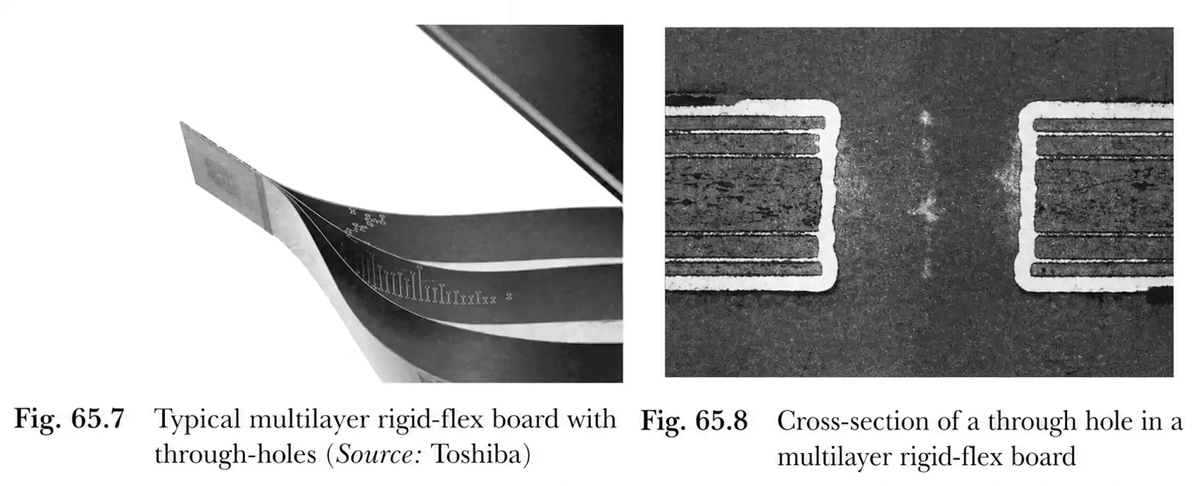
Standard multilayer rigid-flex boards were created to combine rigid and flexible sections into one reliable interconnect structure. In aerospace and other harsh-environment systems, designs often used high layer counts but rarely relied on fine-line circuitry or microvia technology. Instead, they favored wider traces, larger plated through-holes, and heavier copper for better reliability margins.
Medical and industrial products face different design pressures. They often need to:
- fit more circuitry into smaller enclosures
- Reduce connectors and wire harnesses
- improve packaging efficiency
- support dense component layouts
- maintain dependable long-term performance
That combination makes the HDI rigid-flex PCB a practical fit. It offers a way to increase routing density while still supporting a reliability-focused design approach.
For that reason, HDI PCB for medical electronics and rigid-flex PCB for industrial electronics have become important design directions in products where both space savings and performance matter.
What Makes an HDI Rigid-Flex PCB Different?
An HDI rigid-flex PCB is not just a rigid-flex board with tighter routing. It is usually defined by a combination of finer geometry, smaller interconnect structures, thinner materials, and more advanced assembly methods.
Typical HDI rigid-flex characteristics
- Line pitch: below 100 μm
- Hole diameter: below 100 μm
- Base material: 25 μm or thinner adhesiveless thin-copper polyimide
- Copper thickness: often 18 μm or less
- Interconnect type: laser-drilled microvias and blind vias
- Assembly methods: BGA soldering, flip-chip bonding, and other high-density packaging methods
These features do not work independently. As density increases, the entire design and manufacturing system has to improve with it.
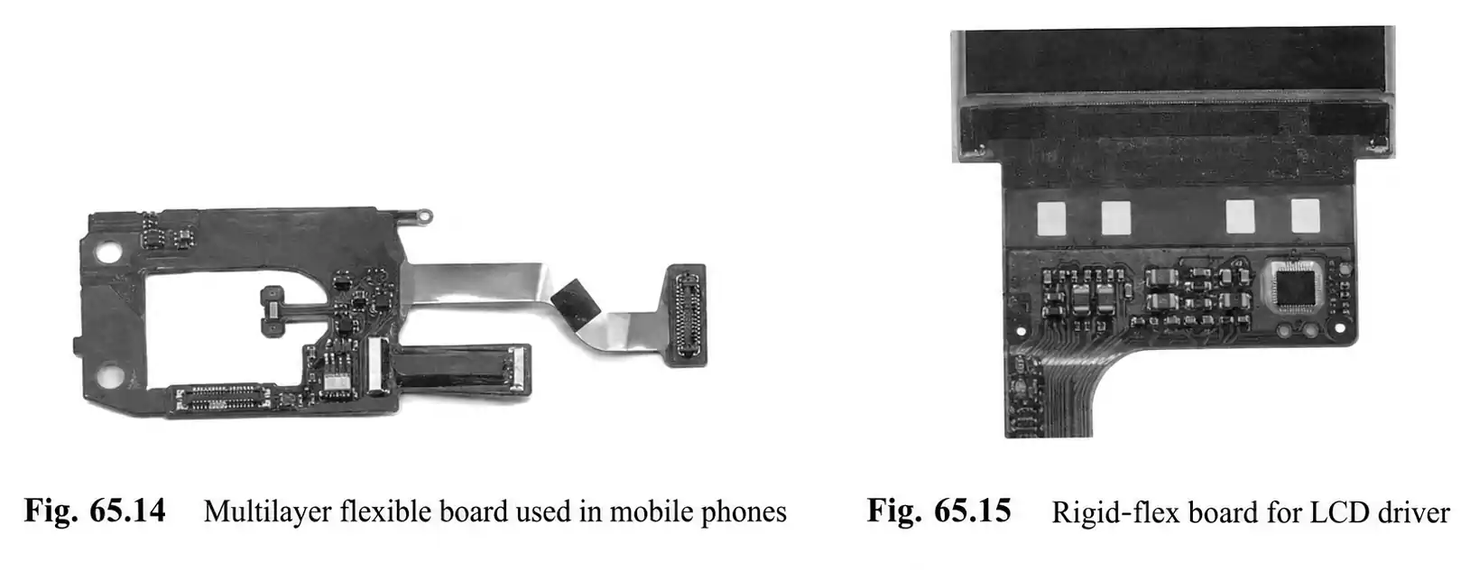
That is especially true in a medical rigid-flex PCB, where routing density, thermal behavior, and long-term reliability must work together. The same is true for an industrial rigid-flex PCB, where process margin and structural durability are often just as important as compact size.
Traditional Rigid-Flex vs. HDI Rigid-Flex
| Main priority | Reliable interconnect in limited space | Higher routing density plus reliability |
| Typical trace/space | Larger geometries | Fine-line routing |
| Hole structure | Conventional plated through-holes | Microvias, blind vias |
| Materials | Standard rigid-flex systems | Thin adhesiveless PI materials |
| Assembly style | Traditional component attachment | BGA, flip-chip, high-density assembly |
| Best fit | Aerospace-style reliability-first designs | Medical and industrial high-density systems |
Why Aerospace Historically Used HDI Rigid-Flex Less Often
High-density rigid-flex structures were not widely used in aerospace for a long time because fine-line and microvia designs were often considered less reliable in harsh operating environments. Aerospace programs typically stayed with more conservative design rules, heavier plated copper, and conventional assembly approaches.
Medical and industrial electronics occupy different positions. They still require strong reliability, but they also face growing pressure for:
- miniaturization
- denser packaging
- more efficient internal interconnects
- fewer discrete interconnect components
As materials, laser drilling, sequential buildup processing, plasma desmear, and high-density assembly methods improved, the HDI rigid-flex PCB became much more viable for these applications.
That is why HDI PCB for medical electronics and rigid-flex PCB for industrial electronics are now practical solutions rather than niche experiments.
Why Adhesiveless Polyimide Materials Matter in a Medical Rigid-Flex PCB
Material choice plays a major role in whether an HDI rigid-flex design succeeds.
For medical and industrial use, materials must provide:
- good thermal resistance
- strong dimensional stability
- compatibility with repeated thermal processing
- support for thinner final constructions
Why are adhesiveless materials preferred
Adhesiveless copper-clad laminates generally offer:
- higher heat resistance
- lower thermal expansion
- Reduced final board thickness
Those properties are especially helpful in a medical rigid-flex PCB or industrial rigid-flex PCB, where dimensional movement during lamination, drilling, plating, and assembly can directly affect yield and reliability.
Why adhesive-based systems can be more limiting
Some adhesive systems introduce additional risk.
For example:
- Acrylic adhesives often provide strong bond strength, but they can have lower heat resistance and higher shrinkage.
- Epoxy adhesive systems may offer better heat resistance, but usually come with different process tradeoffs.
In a high-reliability rigid-flex PCB, adhesiveless systems are often the better long-term choice.
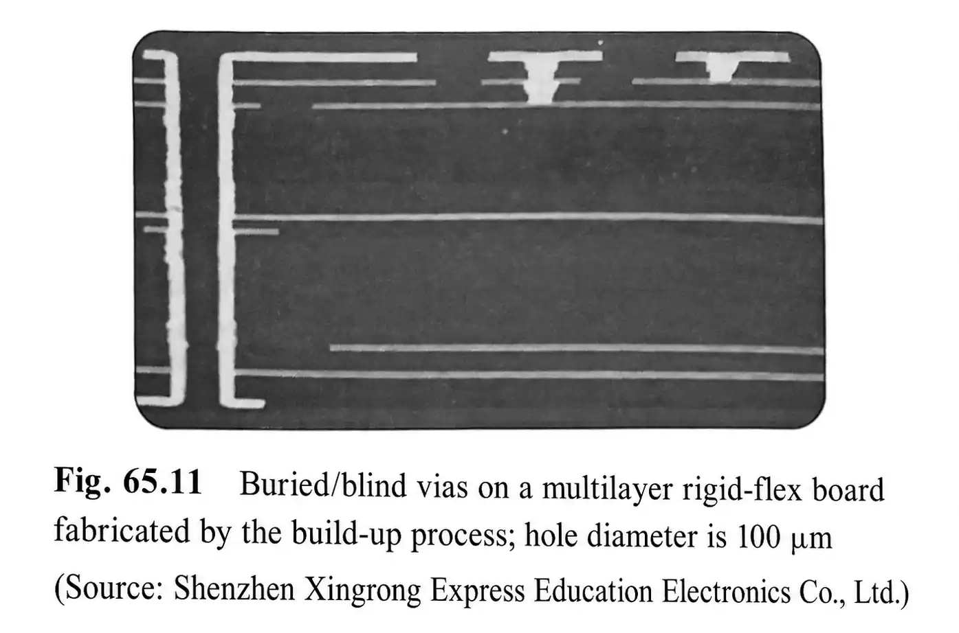
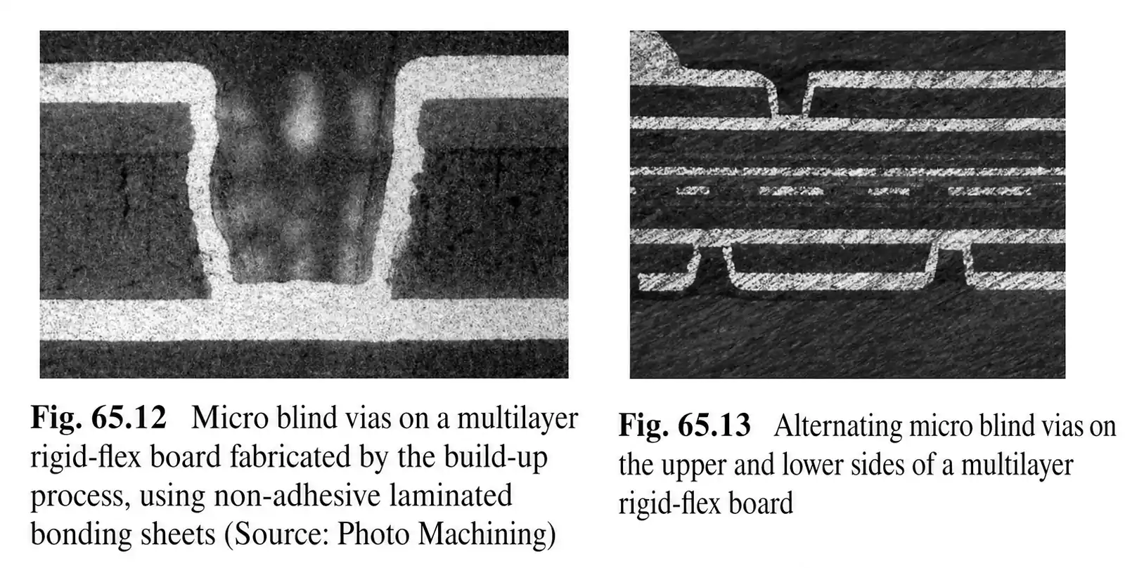
Laser Microvia Rigid-Flex PCB Structures: Microvias, Blind Vias, and Sequential Buildup
Once the trace pitch and hole size move below 100 μm, conventional through-hole structures become less efficient. At that point, microvias and blind vias are not just helpful; they are essential. They become central to the design.
Why laser-drilled vias matter
A laser microvia rigid-flex PCB commonly uses:
- laser-drilled microvias
- laser blind vias
- thin copper plating on via walls
- buildup-style interconnect layers
Why sequential buildup is important
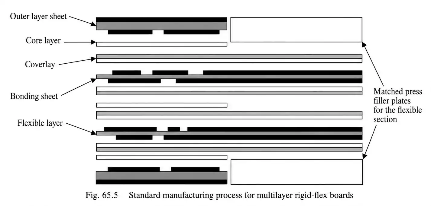
Sequential buildup processing gives designers more flexibility in creating dense interconnect structures layer by layer. A common approach is:
- Laminate adhesiveless materials with bonding layers
- Use CO2 laser drilling to create blind vias
- plate thin copper onto the via wall
- build interconnect density where it is actually needed
The benefit is not simply smaller holes. The real advantage is better interconnect efficiency and more usable routing space in dense areas.
For designs that depend heavily on via density, a blind-via rigid-flex PCB can provide more efficient fan-out and signal escape than a conventional plated-through-hole structure.
Reliability Is Still the Hard Part
High density does not reduce the need for reliability. It increases it.
As interconnect structures become smaller, process control becomes more important. In medical and industrial applications, the challenge is not just making microvias or plated holes small enough. It is making them reliable over time.
Critical reliability factors
1. Pre-baking before drilling
Proper baking helps remove moisture and lowers the risk of failure during drilling, desmear, and plating. In a high-reliability rigid-flex PCB, this is a foundational process step.
2. Desmear process selection
Rigid-flex cannot always use the same desmear process as a standard rigid PCB.
Permanganate chemistry may work well in conventional rigid board fabrication, but in structures that use acrylic adhesive systems, it can cause swelling and reduce plated-hole reliability.
3. Plasma desmear
Plasma etching is generally preferred because it can remove drilling residue without causing obvious damage to adhesive resin layers. That makes it better suited to higher-reliability rigid-flex fabrication.
4. Positive etchback
A commonly recommended positive etchback depth is around 13 μm. This improves cleaning and helps create a more reliable connection between plated copper and the inner layer.
5. Hole wall copper thickness
Industrial-grade applications often call for plated hole wall copper above 25 μm, and in more stringent cases, above 35 μm. Copper thickness remains one of the most important reliability controls in any high-reliability rigid-flex PCB.
Assembly Capability Has to Match the PCB
An HDI rigid-flex PCB is not only a fabrication issue. It is also an assembly issue.
A medical rigid-flex PCB or rigid-flex PCB for industrial electronics is often paired with:
- BGA soldering
- flip-chip bonding
- other high-density packaging methods
That matters because high-density routing does not deliver full value unless the assembly process can support the same level of integration.
A strong design review should ask two questions:
- Can the PCB be fabricated reliably?
- Can the final product also be assembled reliably?
If the answer to the second question is weak, the design may still fail in practice even if the board itself can be built.
Why Consumer Electronics Rules Do Not Translate Directly
Consumer electronics also use dense rigid-flex structures, especially in smartphones, cameras, and compact display modules. Those designs often prioritize:
- low cost
- high production volume
- thin construction
- manufacturing speed
Medical and industrial products do not operate under the same priorities.
They usually care more about:
- long-term reliability
- dimensional consistency
- stable process margins
- plated-hole performance
- structural robustness
While both markets may use high-density rigid-flex boards, the design logic differs between them. Consumer products often optimize density around cost and scale. A medical rigid-flex PCB and an industrial electronics rigid-flex PCB must balance density with reliability and manufacturability.
When an HDI Rigid-Flex PCB Makes Sense
An HDI rigid-flex PCB is usually worth considering when several of these conditions appear at once:
- The available space is extremely limited
- A standard multilayer rigid PCB cannot handle the required routing density
- The design would benefit from fewer connectors or cable assemblies
- high-I/O or fine-pitch packages need more efficient layer-to-layer interconnect
- long-term reliability matters as much as miniaturization
If the main goal is only cost reduction, a more conventional PCB structure may still be the better choice.
For projects that require compact packaging, reduced interconnect complexity, and consistent performance, the HDI rigid-flex PCB often becomes the better long-term solution.
FAQ
When should a medical or industrial product use HDI rigid-flex instead of a standard rigid PCB?
It is a strong option when space is limited, the mechanical structure is complex, or the design needs folding interconnects and higher routing density than a conventional multilayer rigid PCB can support. It is especially useful when reducing connectors and cable assemblies is also a priority.
What is the main difference between HDI rigid-flex and standard rigid-flex?
Standard rigid-flex integrates rigid and flexible regions into a single structure. An HDI rigid-flex PCB adds finer lines, microvias, blind vias, thinner adhesiveless materials, and denser assembly capability. It is essentially a higher-density interconnect version of rigid-flex.
How does HDI technology reduce size?
It improves routing density with finer lines, increases interconnect efficiency with microvias and blind vias, and enables folding or three-dimensional layouts through the rigid-flex structure itself. Together, those changes can reduce both board area and package size.
Why are adhesiveless materials preferred so often?
They usually provide better heat resistance, lower thermal expansion, and thinner final constructions. That makes them better suited to high-density designs that also require strong thermal and dimensional stability.
Can vias be placed in the flex region or bend area?
They should generally be kept out of bend areas whenever possible. Even in flex regions, vias need careful evaluation because bending introduces local stress that can reduce long-term reliability.
Can medical or industrial designs simply follow consumer-electronics rigid-flex practices?
Usually not. Consumer designs are often driven by cost, volume, and thinness. Medical and industrial products place greater emphasis on reliability, process margins, and long-term performance.
Final Thoughts
HDI rigid-flex is not just about finer traces or smaller vias. The real challenge is building a structure in which materials, microvias, lamination, plating, and assembly work together reliably.
That is what makes HDI rigid-flex PCBs such a strong fit for medical and industrial electronics. These applications often require compact packaging, high interconnect density, and stable long-term performance in the same design.
At FastTurn PCB, we see HDI rigid-flex as a practical solution for products where space, complexity, and reliability all matter.
