

An antenna feed network is the system of conductors, transmission lines, and matching elements that delivers RF energy from a transmitter or receiver to one or more antenna elements.
In PCB design, this network does more than carry a signal. It affects impedance matching, insertion loss, phase balance, and overall antenna performance. In array applications, it also controls how power is distributed across multiple elements.
That is why antenna feed network design cannot be reduced to a single 50-ohm trace. Material selection, stackup, feed structure, and layout all influence how efficiently RF energy reaches the antenna.
Key Takeaways
- An antenna feed network is more than a 50-ohm trace.
- Feed performance depends on material, stackup, line structure, matching, and grounding.
- Microstrip and CPWG are not interchangeable.
- A matching network should usually be reserved from the start.
- In antenna arrays, feed topology directly affects phase, loss, and beam behavior.
What Is an Antenna Feed Network?
An antenna feed network is the path that transfers RF energy from a transmitter, receiver, module, or RF front end to one or more antenna elements.
In PCB design, that network may include:
- the RF source output
- a launch or transition
- a transmission line
- a matching network
- a feed point
- ground structures
- power dividers or phase-control sections in array applications
In other words, the feed network is not just the trace. It is the entire RF delivery system between the source and the antenna.
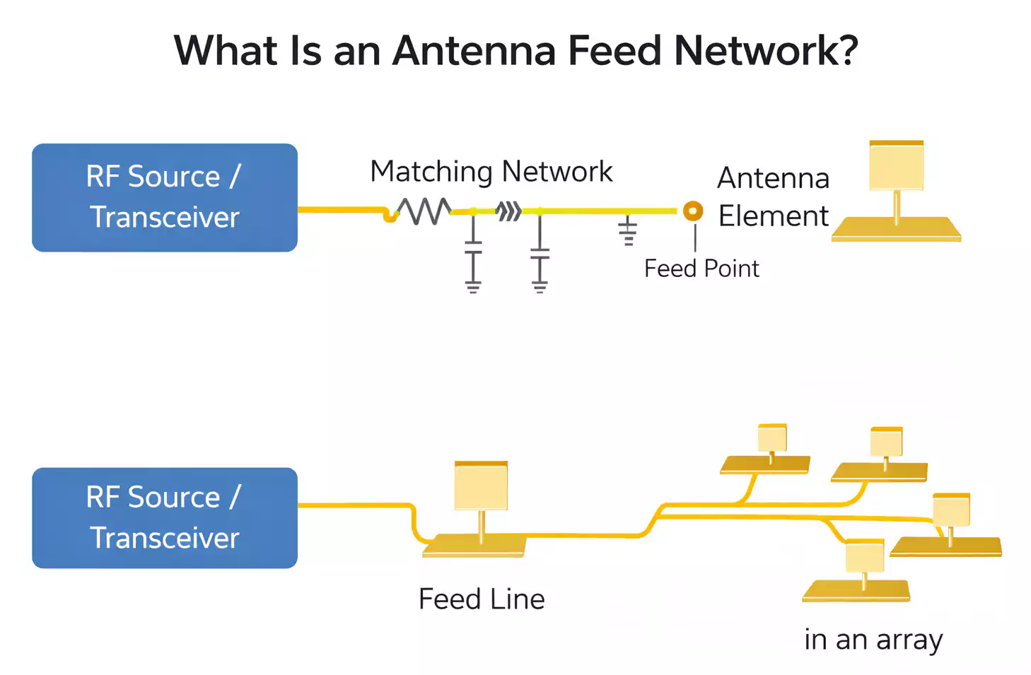
Feed Line vs. Feed Network vs. Feed Point
These terms are often mixed together, but they are not the same.
| Feed line | The transmission path itself, such as microstrip, CPWG, coax, or stripline |
| Feed network | The larger RF path that may include feed line, matching, transitions, dividers, and grounding structures |
| Feed point | The physical location where energy enters the antenna element |
That distinction matters because many layout problems arise from treating the entire feed network as a single controlled-impedance trace.
Why a 50-Ohm Trace Is Not Enough
A 50-ohm trace does not mean the antenna is matched.
It only means the transmission line is designed for a target characteristic impedance under a specific stackup and geometry. The antenna still has its own input impedance, and that value can shift with frequency, nearby metal, enclosure conditions, ground structure, trace length, matching components, and manufacturing variation.
So a correct feed line does not guarantee a tuned antenna system. Final matching still depends on the antenna, the layout, and the product environment.
The Main Functions of an Antenna Feed Network
An antenna feed network typically has three main functions: transferring RF energy, supporting impedance matching, and, in array designs, controlling power and phase distribution.
1. Transfer RF Energy Efficiently
The first job is to deliver RF energy from the source to the antenna with minimal loss, reflection, or unintended radiation.
In practice, that depends on several factors:
- line length
- material loss
- transition quality
- impedance continuity
- bend geometry
- nearby noise sources
2. Support Impedance Matching
Most PCB antennas are not perfectly matched by default. A matching network is often needed to improve return loss and power transfer at the target frequency.
Common matching topologies include:
- L network
- Pi network
- T network
For many PCB antenna designs, a Pi network footprint is a practical starting point because it gives more flexibility during tuning.
3. Control Power and Phase in Arrays
In array antennas, the feed network also determines how RF power is distributed across the antenna elements.
That directly affects:
- phase consistency
- amplitude balance
- gain
- beam direction
- side lobe behavior
- overall array efficiency
Common Feed Structures Used on PCBs
The feed structure directly impacts loss, routing flexibility, and manufacturability.
Microstrip
Microstrip is one of the most common feed structures in PCB antenna design. It typically uses an outer-layer trace with a reference ground plane below it.
Advantages
- simple to implement
- easy to connect to matching components
- widely used in wireless PCB layouts
Limitations
- sensitive to nearby layout changes
- easily affected by adjacent ground copper or metal objects
- may provide less isolation in dense RF sections
Grounded Coplanar Waveguide (CPWG)
CPWG uses an outer-layer trace with grounded copper on both sides. It is widely used in compact RF layouts and mixed-signal boards.
Advantages
- better isolation
- more controlled field distribution
- Often better suited for noisy mixed-signal environments
- can support practical trace widths on thicker boards
Limitations
- Impedance depends on both trace width and ground spacing.
- Spacing must remain consistent.
- Geometry often requires a field solver for accurate design.
Stripline
Stripline routes the signal inside the PCB, between ground planes.
Advantages
- strong shielding
- better protection from external interference
Limitations
- less convenient for matching and tuning
- usually not used as the final feed structure at the antenna feed point
- Transitions to outer-layer antenna structures require careful design.
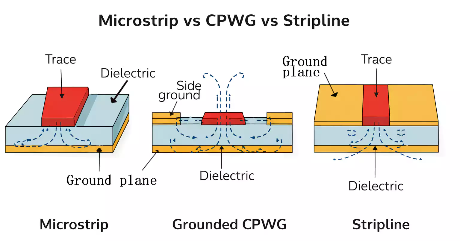
Microstrip vs. CPWG
This is one of the most important design choices in PCB antenna feed routing.
| Routing layer | Outer layer | Outer layer |
| Reference | Ground plane below | Ground plane below plus side grounds |
| Isolation | Moderate | Better |
| Geometry sensitivity | High | High |
| Typical use | Simple RF traces, PCB antennas | Compact RF layouts, dense mixed-signal boards |
| Design complexity | Lower | Higher |
A microstrip and a CPWG with the same target impedance do not use the same width.
Once the side-ground copper is close enough, the line no longer behaves like a pure microstrip. That changes the field pattern and the impedance.
Why Material Selection Matters
PCB material properties directly impact antenna feed network performance.
The most important ones include Dk, Df, dielectric thickness consistency, copper roughness, fabrication tolerance, and moisture sensitivity. Together, they affect impedance control, insertion loss, and tuning stability.
When Material Choice Becomes More Critical
Material selection matters more as RF demands increase, especially when frequency is higher, feed lines are longer, bandwidth is narrower, phase stability is more important, or production consistency is tighter.
For shorter feeds at lower frequencies, standard materials may be sufficient. At higher frequencies, however, the feed network becomes much more sensitive to substrate quality and manufacturing variation.
Stackup Design for Antenna Feed Networks
Stackup is not just a manufacturing detail. It directly affects feed impedance, loss, return path behavior, and layout stability.
2-Layer Boards
A 2-layer board can work for simple wireless products, especially if:
- The RF section is small.
- The bottom layer remains mostly solid ground.
- Noise sources are limited.
Pros
- lower cost
- simpler construction
Cons
- less isolation
- more layout tradeoffs
- harder to manage mixed-signal interference
4-Layer Boards
For many RF PCB designs, a 4-layer board is a better starting point.
A common arrangement is:
| L1 | RF traces, antenna, matching parts |
| L2 | Solid ground plane |
| L3 | Power and low-noise routing |
| L4 | Digital and support signals |
This structure usually gives better:
- reference continuity
- impedance control
- RF/digital separation
- tuning stability
6-Layer and Higher
More complex systems may need 6-layer or higher stackups, especially when RF, digital, power, and high-speed signals must coexist.
In those cases, the goal is to keep the RF path clean while pushing noisy routing deeper into the stack.
Grounding, Return Path, and Keep-Out Rules
Good antenna feed design depends heavily on understanding that the feedline region and the radiating region are distinct.
Feed Line Region
The feed line usually wants:
- a stable reference ground
- controlled impedance
- minimal discontinuities
- a clean return path
Antenna Region
The antenna element usually needs a keep-out area that avoids:
- copper pours
- stitching vias inside the wrong area
- shielding cans
- batteries
- displays
- screws
- metal brackets
- noisy components
That is why a feed line may need a continuous ground below it, while the radiator itself may need copper removed or limited around it.
Matching Networks in PCB Antenna Design
A matching network is often what separates a marginal antenna design from a stable one.
Why Reserve a Matching Network
Even when the first prototype looks acceptable, antenna performance can shift in production due to:
- dielectric tolerance
- copper thickness variation
- assembly differences
- enclosure changes
- nearby layout changes
- stackup changes
For that reason, many RF designers reserve a Pi network from the start.
Common Matching Topologies
| L network | Simple matching with fewer components |
| Pi network | Flexible tuning, common in PCB antenna designs |
| T network | Useful when a different tuning range or topology is needed |
Ground Under Matching Components
In some designs, ground is removed locally under the matching network to reduce parasitic capacitance and inductance.
That does not mean the full feed region should lose its reference plane. It is a local optimization used only around the matching section.
Feed Network Topologies for Antenna Arrays
Once a design moves from a single antenna to an array, the feed network becomes a system-level decision.
Corporate Feed
Corporate feed divides power in parallel across multiple branches.
Strengths
- good control of amplitude distribution
- easy to create equal excitation
- suitable for many array layouts
Tradeoffs
- uses more board area
- Feed paths can become longer
- Loss can increase at higher frequencies
Series Feed
The series feed passes RF power through the array in sequence.
Strengths
- compact layout
- efficient in some designs
- requires less routing area
Tradeoffs
- introduces natural phase progression
- Often has a narrower bandwidth
- less flexible for some array requirements
H-Tree Feed
H-tree feed is useful when an equal electrical path length is important.
Strengths
- balanced branching structure
- supports phase consistency
- scales well in array layouts
Tradeoffs
- still requires careful divider design
- can become layout-intensive as the array size grows
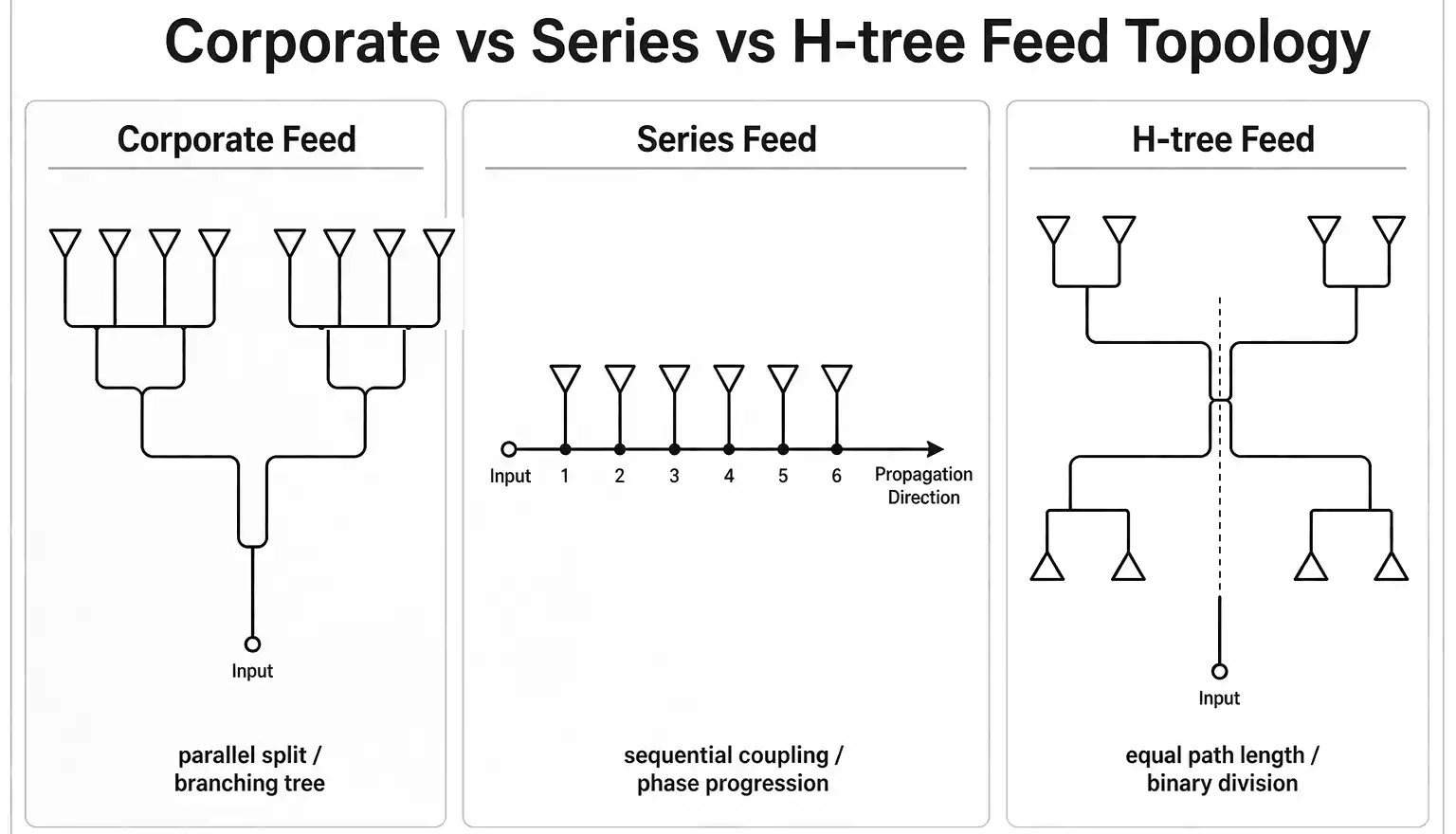
Quick Comparison
| Corporate | Controlled amplitude distribution | More area and higher feed loss |
| Series | Compact arrays | Phase and bandwidth constraints |
| H-tree | Equal-length distribution | Higher layout complexity |
Simulation, Measurement, and Tuning
Antenna feed networks should be verified by measurement, not solely by layout.
Why Layout Alone Is Not Enough
Real PCB performance is affected by fabrication tolerance, component parasitics, enclosure effects, interconnects, and the surrounding antenna environment. As a result, a layout that looks correct in design may still require tuning in hardware.
A Practical Tuning Flow
A practical workflow is straightforward:
- define the stackup and target impedance
- reserve matching pads
- Route the feed with controlled geometry.
- build the prototype
- measure S11 and impedance
- Adjust the matching network with Smith chart data.
- Recheck performance in the final product condition
For that reason, matching values from a reference design should be treated as a starting point, not a final solution.
Common Mistakes in Antenna Feed Network PCB Design
These mistakes keep showing up in real projects.
Design Mistakes to Avoid
- assuming a 50-ohm line means the antenna is matched
- Treating microstrip and CPWG as interchangeable
- routing the feed across a split or slot
- placing noisy circuitry too close to the antenna feed
- violating antenna keep-out rules
- using abrupt width changes
- Adding stubs or unnecessary test pads to the RF path
- removing the matching network because one prototype seemed acceptable
- ignoring stackup variation during tuning
- choosing an array feed topology based only on convenience
FAQ
What is an antenna feed network in PCB design?
An antenna feed network is the RF path that transfers energy from the source to the antenna. On a PCB, it usually includes the feed line, matching network, and ground reference.
Is a 50-ohm trace enough for good antenna performance?
No. A 50-ohm trace defines the transmission line impedance, not the antenna input impedance. Final performance still depends on the antenna, layout, and product environment.
Should I reserve a matching network on the PCB?
In most cases, yes. A reserved matching network provides greater flexibility during tuning and helps compensate for variations in layout, materials, and enclosure conditions.
Which feed structure is better for PCB antennas: microstrip or CPWG?
It depends on the design. Microstrip is simpler, while CPWG often provides better isolation and is commonly used in compact RF layouts.
Why does stackup matter in antenna feed design?
Stackup affects impedance, loss, and return path behavior. The same trace can perform differently on a different layer structure or material system.
Final Thoughts
Antenna feed network PCB design is not just about routing RF energy to an antenna. It is about controlling impedance, loss, grounding, and phase behavior across the full RF path.
In practice, good results come from getting the fundamentals right early: material, stackup, feed structure, matching, and layout. For single-antenna boards, that usually means a short and controlled feed with a stable ground reference. For array designs, it also means choosing a feed topology that fits the electrical and mechanical requirements.
When these decisions are made correctly at the PCB design stage, antenna tuning becomes more predictable, and production results are easier to control.
For projects moving from RF design into fabrication, FastTurnPCB is one option to consider.