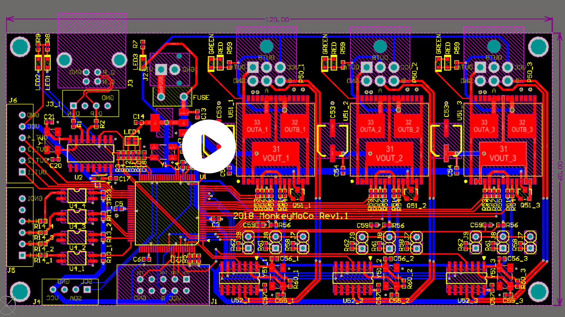
4-Layer PCB Layout in 5 Simple Steps – Stackup, Routing & Best Practices
Learn how to design a professional 4-layer PCB layout in 5 simple steps. This video covers everything from layer stackup and signal integrity to proper routing techniques and grounding strategies. Whether you're using Altium, KiCad, or another EDA tool, this tutorial explains the key principles of 4-layer PCB design for improved performance and EMC compliance.
✅ What’s included:
- 4-layer PCB stackup structure explained
- Best routing practices for signal, power, and ground planes
- Via placement and trace width considerations
- Design rules for multilayer PCBs
- Common mistakes to avoid in 4-layer layout
Perfect for electronics engineers, PCB designers, and students working on high-speed or compact circuit designs.