What Is A Thick Copper PCB?

Thick copper PCB solutions for high-current applications

As a leading China flex PCB supplier, we specialize in high-quality flex circuit manufacturing—from rapid-turn prototyping to full-volume flexible PCB fabrication. Upload your Gerber files now for a fast, reliable quote.

Customer Satisfaction Rate
0 %
Annual Ordering Customers
0 +
Countries
0 +
On-time delivery rate
0 %

China Thick Copper PCB Manufacturer

At Fast Turn PCB, we specialize in producing robust, high-current printed circuit boards with copper thicknesses ranging from 2oz to over 20oz. Designed to handle extreme current loads, improve heat dissipation, and ensure long-term durability, our thick copper PCBs are ideal for power electronics, automotive systems, industrial controls, and military applications.

Whether you need quick-turn prototypes or full-scale production, our
advanced manufacturing capabilities and experienced engineering team
ensure that your custom heavy copper PCB meets the highest standards for
performance and reliability. With precise etching, multilayer support, and
full compliance with international quality certifications, we deliver results
that power your innovations.

What Is A Thick Copper PCB?

A Thick Copper PCB—also known as a Heavy Copper PCB—is a printed circuit board that features significantly thicker copper layers than standard PCBs. While conventional PCBs typically use 1oz (35μm) copper thickness, thick copper PCBs use copper layers of 2oz (70μm) or more, often reaching up to 20oz (700μm) or higher for specialized applications.

These boards are engineered to carry higher current loads, provide superior thermal management, and ensure enhanced mechanical strength, especially in harsh environments or power-intensive systems.

Typical Copper Thickness Ranges

Key Characteristics

Where It’s Used

Applications

Manufacturing Process

01. Engineering Review & DFM Check

Every project begins with a thorough design review and DFM (Design for Manufacturability) analysis to ensure optimal layout, copper weight compatibility, and manufacturability.

02. Material Selection

We select high-Tg, high-thermal-conductivity base materials suitable for heavy copper etching and high-power applications.

03. Inner Layer Imaging & Etching

For multilayer designs, inner layers are imaged and etched with extra care to manage wide traces and thick copper distribution accurately.

04. Lamination

Multilayer boards are pressed under high temperature and pressure using advanced vacuum lamination to ensure uniform bonding of thick copper layers.

05.Drilling & Hole Plating

Holes are drilled and electroplated with heavy copper using controlled plating techniques to maintain via integrity and current-carrying capacity.

06. Outer Layer Imaging, Etching & Plating

Outer copper layers are patterned and etched, followed by precise plating to achieve the final copper thickness as specified.

07. Solder Mask & Surface Finish

A high-temperature-resistant solder mask is applied, followed by a surface finish such as ENIG, HASL, or OSP for improved solderability.

08.Routing, V-Cut, and Mechanical Processing

The boards are routed, scored, or CNC machined as per design, ensuring smooth edges and tight tolerances.

Quality Control

Automated Optical Inspection (AOI) for inner and outer layers

X-ray Inspection for multilayer alignment and plated through-hole quality

X-ray Inspection for multilayer alignment and plated through-hole quality

Cross-section Analysis for copper thickness and via quality verification

ISO & UL Certified Processes, ensuring international compliance

RoHS & REACH Compliance, as required for global applications

Support & Services

Engineering Assistance

Rapid Prototyping

Scalable Production

Reliable Delivery

Custom Capabilities

FAQ

Q:What is a thin copper PCB? What is its main use?

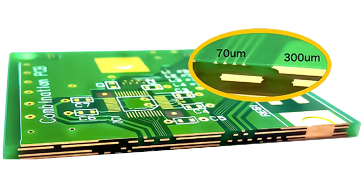
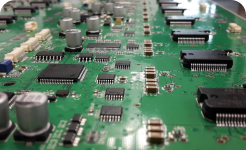
Thick copper printed circuit boards refer to printed circuit boards with copper foil thickness far exceeding conventional standards.

Their primary purpose is to meet the requirements of high current density, high thermal conductivity, and high mechanical strength.

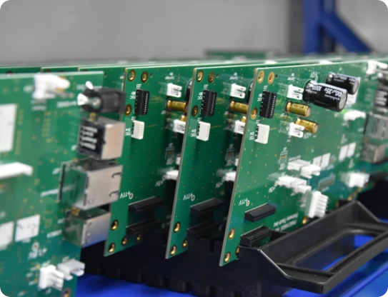
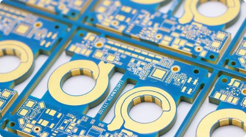
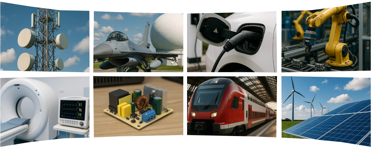
This type of circuit board is commonly used in power electronics, automotive electronics, industrial control, communication base stations, aerospace and other fields to ensure stable operation in high power and harsh environments.

Q:What is the typical copper foil thickness for thick copper PCBs?

Flex PCBs are primarily made from polyimide (PI) or polyester (PET) substrates with copper foil layers. We also use adhesiveless laminates for high-reliability applications. Coverlays, stiffeners (FR4 or stainless steel), and surface finishes (ENIG, OSP) are added depending on the design.

Q:What special processes and techniques are required to manufacture thick copper PCBs?

Lead times depend on complexity and quantity:

  • Prototype Flex PCBs: 3–7 business days
  • Production Runs: 7–20 business days

Expedited options are available for urgent projects — contact us for a custom quote.

Q:What are the advantages of thick copper PCBs in high-power applications?
  • Flex PCBs use flexible base materials and are designed to bend, fold, or twist during use.
  • Rigid PCBs are built on FR4 substrates and are not designed for movement.

Flex PCBs save space, reduce weight, and improve durability in dynamic environments.

Q:How to ensure the quality and reliability of thick copper PCBs?

Absolutely. Our engineering team offers free DFM reviews, helping you optimize your design for manufacturability, cost efficiency, and long-term reliability. Upload your Gerber files, and we’ll evaluate them before production begins.

Get In Touch