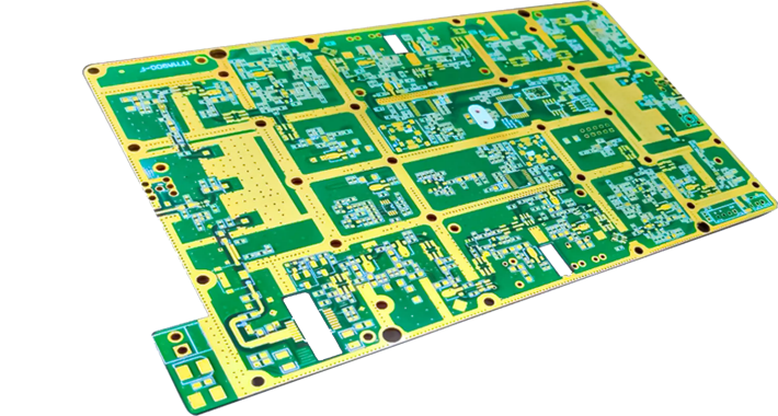
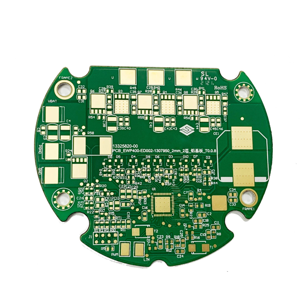
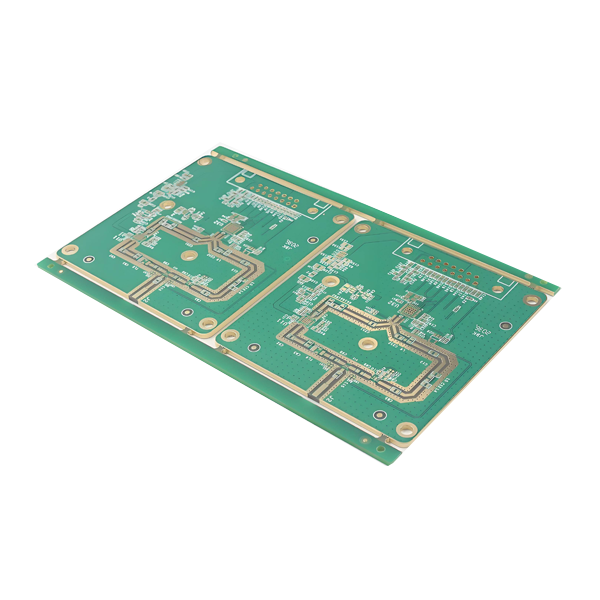
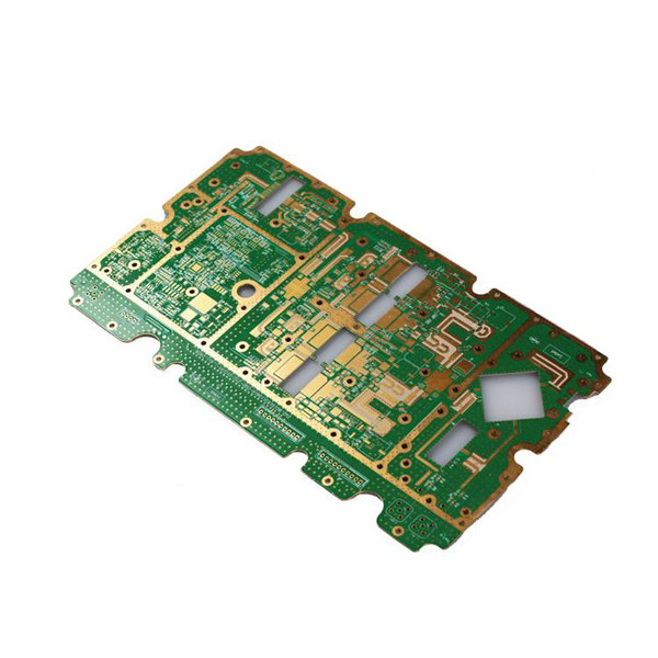
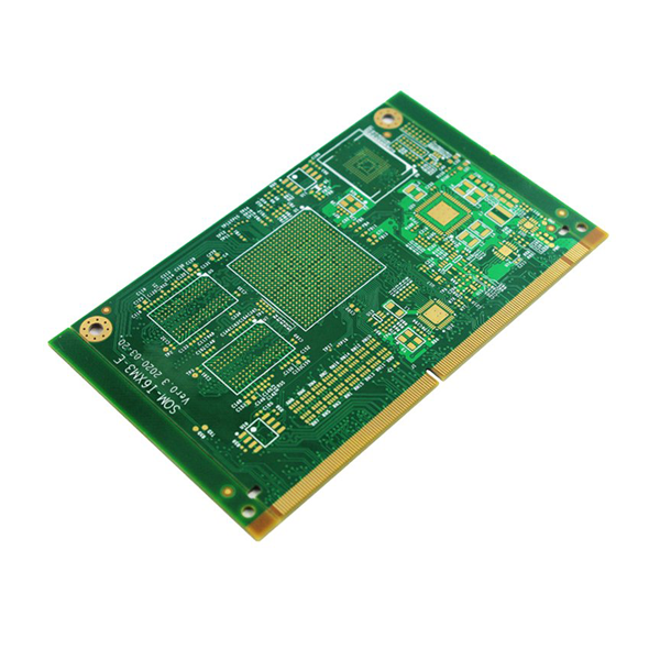
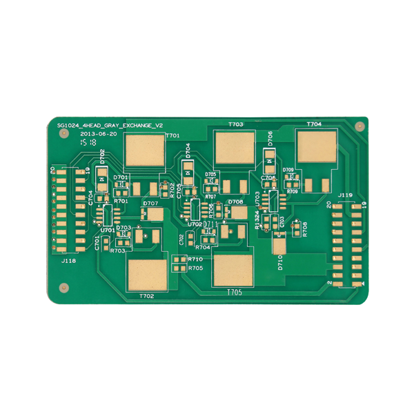
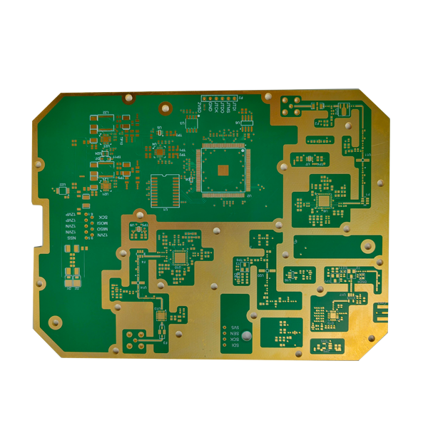
High Frequency PCBs,
High frequency printed circuit board is a type of circuit board designed specifically to meet the requirements of high-frequency signal transmission.
They use special substrates and manufacturing processes to ensure excellent electrical performance and stability at high frequencies.
This type of circuit board has a wide range of applications in wireless communication, radar systems, satellite communication, high-speed data transmission, and other fields.