HDI PCB Manufacturer

Advanced HDI PCB Fabrication & Assembly

As a trusted HDI PCB manufacturer in China., we deliver precision high-density interconnect boards—from quick-turn prototypes to complex multilayer fabrication. Upload your Gerbers now for a fast, accurate quote.

HDI PCB Services

HDI PCBs

HDI PCBs use micro blind hole/buried blind hole technology to achieve interconnection between different copper layers inside.Compared to traditional through-hole connections, HDI PCBs can achieve higher processing speeds and more functions, while reducing the surface area and thickness of circuit boards, making electronic devices more beautiful and compact.

HDI PCBs have a wide range of applications in fields such as data communication, automotive, and consumer electronics, especially in miniaturized electronic devices such as smartphones, tablets, and wearable devices.

HDI Overview

An HDI (High-Density Interconnect) PCB uses blind vias, buried vias and laser-drilled microvias to push routing density and signal integrity to the limit.

With sequential lamination and via-fill/plug processes, it delivers more channels, shorter paths and lower crosstalk in a compact footprint.

Board-area savings

Microvias and buried vias cut PCB size by over 30%, boosting compactness.

Flexible multilayer design

Stack 4–32 layers freely for complex layouts and high I/O density.

High-speed performance

Short traces and uniform impedance control support differential rates up to 28 Gbps.

EMI/EMC optimization

Shorter return paths and uniform layer distribution effectively reduce EMI/EMC risks.

Product Showcase

Capabilities

Capability Parameter
Min. Line Width/Space 2.5/2.5
Max. Layer Count 20
Min. CCL Thickness 50um
Min. Build-Up Thickness 35um
Min. Microvia Design 100um/200um
Min. Finished PTH Size 0.15mm
Impedance Control Impedance Tolerance:+/-5om or +/-10%
RoHs Certification RoHs Certification
Lead Free Compliance Available
Green Material-H/F Available
Copper filled Microvia Available
ELIC Level 18 Layers

What they say?

testimonial-3-1-img.jpg
The signal integrity and precision of these HDI boards are unmatched—we saw immediate improvements in our RF module performance.
testimonial-3-2-img.jpg
Their HDI PCB solutions helped us miniaturize our control units without compromising thermal stability or durability. Excellent reliability!
testimonial-3-3-img.jpg
From layout consultation to final delivery, the service was professional and fast. The HDI stack-up met all aerospace compliance requirements.

Industry Applications

FAQ

High density interconnect printed circuit board is a circuit board that uses micro blind hole/buried blind hole technology to achieve high-density interconnect between different copper layers inside.

 Compared with traditional PCBs, HDI PCBs have higher wiring density and smaller volume, which can meet the demand for electronic products to develop towards lightweight and high-performance.

 In addition, HDI PCBs also exhibit superior performance in signal transmission speed, electrical performance, and reliability.

The manufacturing process of HDI PCBs involves multiple key technologies, among which laser drilling technology, electroplating filling technology, and lamination technology are the most critical.

HDI PCBs are widely used in various fields, especially in miniaturized electronic devices such as smartphones, tablets, and wearable devices.

 In addition, with the increasing demand for high-performance and high reliability circuit boards in fields such as automotive electronics, medical electronics, and aerospace

HDI PCBs achieve high-density interconnection between different copper layers inside by using micro blind hole/buried blind hole technology and stacking technology.

 Micro blind hole/buried blind hole technology enables wiring to be carried out in a smaller space, thereby increasing wiring density.

 At the same time, multi-layer technology stacks multiple thin circuit boards together through multiple lamination and drilling processes, further increasing the number of wiring layers and the installation space for electronic components, thereby improving the overall wiring density.

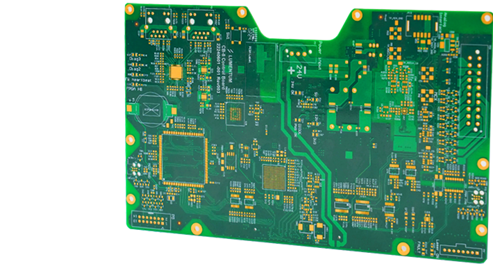
HDI PCBs have multiple special requirements in the design and manufacturing process.

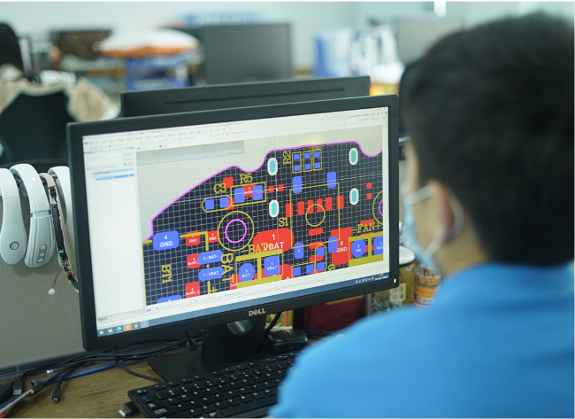
 Firstly, due to the high wiring density of HDI PCBs, advanced EDA software is required for precise wiring during design.

 Secondly, it is necessary to strictly control various process parameters during the manufacturing process, such as the aperture size of laser drilling and the filling quality of electroplating holes, to ensure the quality and performance of the product.

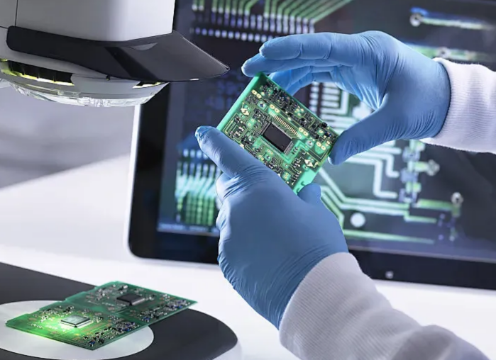
 In addition, HDI PCBs also have special requirements for testing and inspection, requiring high-precision testing equipment and methods for electrical performance testing, reliability testing, etc.

Put your parts
into production today

All information and uploads are secure and confidential.