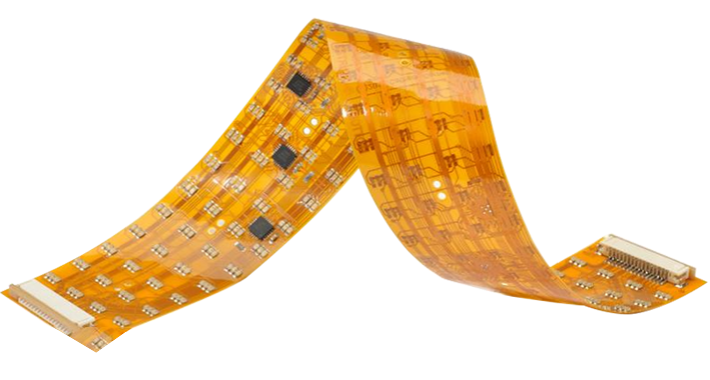
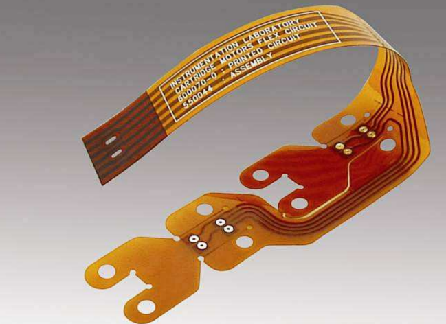
Flex PCB Manufacturer
Rapid Prototype & Volume Flex PCB Fabrication Services
As a leading China flex PCB supplier, we specialize in high-quality flex circuit manufacturing—from rapid-turn prototyping to full-volume flexible PCB fabrication. Upload your Gerber files now for a fast, reliable quote.


What is Flex PCB Manufacturing ?
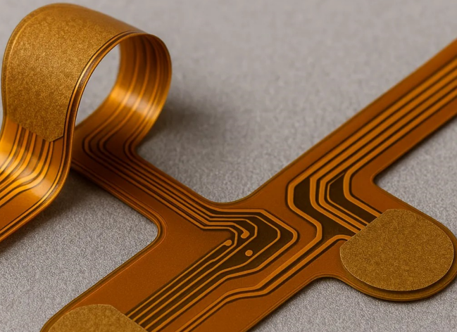
Flex PCB manufacturing refers to the process of designing and fabricating flexible printed circuit boards (FPCs) — electronic interconnects made from flexible substrates like polyimide or polyester. Unlike rigid PCBs, Flex PCBs can bend, fold, or twist without breaking, making them ideal for compact, dynamic, or curved electronic applications.
Key Characteristics of Flex PCBs
- Flexible Substrate Materials: Typically polyimide or PET, offering excellent thermal stability and flexibility.
- Compact Design: Enables 3D routing, reducing space and weight in electronic devices.
- Durability: High resistance to vibration and movement over time, making them suitable for dynamic environments.
- Customization: Easily tailored to meet the electrical and mechanical requirements of specific applications.
The Flex PCB Manufacturing Process Includes
- Flexible Substrate Materials: Typically polyimide or PET, offering excellent thermal stability and flexibility.
- Compact Design: Enables 3D routing, reducing space and weight in electronic devices.
- Durability: High resistance to vibration and movement over time, making them suitable for dynamic environments.
- Customization: Easily tailored to meet the electrical and mechanical requirements of specific applications.

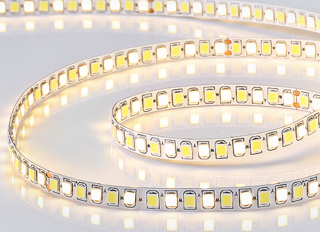
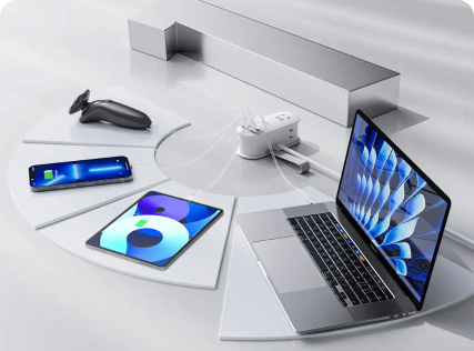
Applications of Flex PCB Manufacturing:
- Wearable Devices
- Automotive Electronics
- Medical Equipment
- Aerospace and Military Systems
- Consumer Electronics (Foldable Phones, Cameras, etc.)
By leveraging Flex PCB manufacturing, engineers and product developers can design more compact, durable, and innovative products — especially where space constraints, movement, or weight reduction are critical.
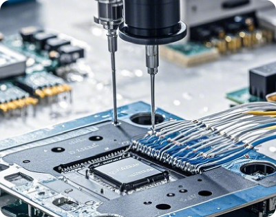
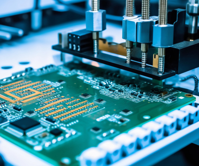
Our Core Advantages in Flex PCB Manufacturing
As a professional Flex PCB manufacturer, we combine advanced engineering, high-precision fabrication, and responsive customer support to deliver reliable and customized flexible circuit solutions. Here’s what sets us apart:
Step 1
High-Quality Materials for Maximum Reliability
We use premium polyimide substrates and rolled annealed (RA) copper foils, which ensure excellent flexibility, heat resistance, and mechanical endurance. These materials meet RoHS, UL, and IPC-6013 Class 3 standards — ideal for mission-critical applications in aerospace, medical, and automotive electronics.
Step 2
Advanced Manufacturing Capabilities
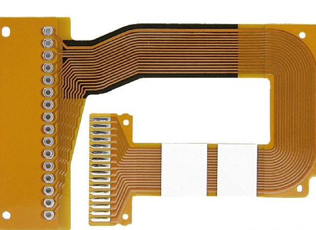
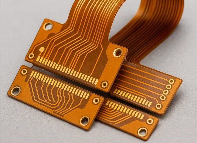
- Single-sided, double-sided, and multilayer flex PCBs
- Rigid-Flex PCB integration for complex designs
- Fine-line circuitry, tight bend radii, and HDI (High-Density Interconnect) support
- Custom stack-ups and stiffener options for enhanced mechanical strength
Our production facilities are equipped with automated optical inspection (AOI), laser drilling, vacuum lamination, and controlled impedance testing, ensuring tight process control and consistent output quality.

Step 3
Engineering Support from Concept to Delivery
We provide Design for Manufacturability (DFM) guidance to help clients
optimize their flex PCB layouts for performance and cost-effectiveness.
Our in-house engineers collaborate closely with you during prototyping,
production, and even post-delivery phases.
Need help with design files or Gerber review? We offer free file audits and
engineering consultation to minimize rework and reduce time to market.
Step 4
Certified Quality and Compliance
Our manufacturing processes follow strict ISO 9001:2015, ISO 13485, and IPC/WHMA-A-620 standards. We implement 100% E-test, mechanical inspection, and thermal stress testing to ensure product integrity before shipping.
Step 5
Fast Turnaround & Flexible Order Quantities
Whether you need rapid prototyping or volume production, we offer flexible lead times — as fast as 24–48 hours for prototypes, and scalable options for mass production. Small batch orders are welcome.
Step 6
Industry-Specific Expertise
Our Flex PCBs are trusted by global clients in:
- Medical Devices (wearable monitors, diagnostic tools)
- Automotive Systems (sensors, control units)
- Consumer Electronics (foldable phones, cameras)
- Industrial Automation (robotics, sensors)
- Aerospace & Defense (avionics, rugged systems)
With a focus on precision, quality, and speed, we are your trusted partner for complex and custom Flex PCB manufacturing.
Flex PCB Design and Manufacturability Guidelines
Designing a high-performance Flex PCB requires careful attention to both electrical performance and mechanical reliability. At our facility, we support clients with Design for Manufacturability (DFM) best practices to ensure your flex circuit is both functional and production-ready.Here are the essential design guidelines to help you achieve optimal results.
Bend Radius and Flexibility
To avoid mechanical stress and copper cracking during repeated flexing,
always follow minimum bend radius rules:
Static Flexing: Minimum bend radius = 6× the total board thickness
Dynamic Flexing: Minimum bend radius = 12× or more of board thickness
Use rolled annealed (RA) copper for better ductility in dynamic applications
Tip: Avoid placing vias or solder joints in areas that will flex repeatedly.
Trace Routing Techniques
- Route traces perpendicular to the bend when possible to reduce stress
- Use curved traces instead of sharp angles to prevent stress fractures
- Maintain consistent trace width and spacing to avoid impedance mismatches
- Use tear-drop pads to strengthen pad-to-trace transitions
Controlled impedance? Use uniform trace geometry and maintain proper dielectric spacing in multilayer designs.
Layer Stack-Up And Construction
- For multilayer flex PCBs, keep symmetrical stack-ups to prevent warping
- Avoid placing copper on both sides in highly flexed regions (prefer single-layer in bend areas)
- Include stiffeners (FR4 or stainless steel) in connector or component regions to add mechanical support
Common stack-up configurations include:
- Single-sided Flex
- Double-sided Flex with plated-through holes
- Multilayer Flex (3+ layers)
- Rigid-Flex combinations
Pad, Via, And Component Placement
- Keep components and vias away from bend areas
- Use anchor pads or adhesive backing for heavier components
- Reinforce solder joints using coverlay openings instead of solder mask
- Laser-drilled microvias are ideal for HDI flex designs where space is limited.
Controlled impedance? Use uniform trace geometry and maintain proper dielectric spacing in multilayer designs.
Material
- Polyimide film (PI) is the preferred base material for its flexibility and thermal resistance
- Adhesiveless laminates can improve reliability and reduce thickness
- Stiffeners (e.g., FR4, PI, or stainless steel) should be carefully specified in mechanical drawings

Layer Stack-Up And Construction
- For multilayer flex PCBs, keep symmetrical stack-ups to prevent warping
- Avoid placing copper on both sides in highly flexed regions (prefer single-layer in bend areas)
- Include stiffeners (FR4 or stainless steel) in connector or component regions to add mechanical support
Common stack-up configurations include:
- Single-sided Flex
- Double-sided Flex with plated-through holes
- Multilayer Flex (3+ layers)
- Rigid-Flex combinations
Benefits of DFM in Flex PCB Design

Reduces production delays and errors
The customer provides part of the materials (e.g., components), while the manufacturer handles the rest.
The manufacturer handles everything – from PCB fabrication and component sourcing to assembly, testing, and delivery. The customer only provides design files.
The customer provides part of the materials (e.g., components), while the manufacturer handles the rest.
Whether you’re designing a simple single-layer flex circuit or a complex multilayer rigid-flex board, our engineering team is here to help you apply proven DFM strategies from day one.
Need help reviewing your Gerber files or stack-up? Contact our engineers for a free DFM consultation.
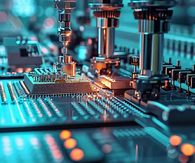
Flex PCB Manufacturing Process Overview
The manufacturing of Flexible Printed Circuit Boards (Flex PCBs) involves a series of high-precision processes designed to ensure electrical performance, mechanical flexibility, and long-term reliability. Below is an overview of the typical flex PCB fabrication workflow — from raw materials to fully tested boards.
01.Material Preparation & Cutting
Next, microvias and through-holes are created to connect different layers or accommodate component pins. This is done using laser drilling for microvias or mechanical drilling for larger holes. Precision and cleanliness are critical to ensure high-quality interconnects. Proper via wall quality ensures better plating adhesion and long-term reliability.
02.Drilling (Via and Hole Creation)
Next, microvias and through-holes are created to connect different layers or accommodate component pins. This is done using laser drilling for microvias or mechanical drilling for larger holes. Precision and cleanliness are critical to ensure high-quality interconnects. Proper via wall quality ensures better plating adhesion and long-term reliability.
03.Circuit Pattern Imaging
Next, microvias and through-holes are created to connect different layers or accommodate component pins. This is done using laser drilling for microvias or mechanical drilling for larger holes. Precision and cleanliness are critical to ensure high-quality interconnects. Proper via wall quality ensures better plating adhesion and long-term reliability.
04.Copper Etching
Next, microvias and through-holes are created to connect different layers or accommodate component pins. This is done using laser drilling for microvias or mechanical drilling for larger holes. Precision and cleanliness are critical to ensure high-quality interconnects. Proper via wall quality ensures better plating adhesion and long-term reliability.
05.Layer Lamination (for Multilayer Flex or Rigid-Flex)
Next, microvias and through-holes are created to connect different layers or accommodate component pins. This is done using laser drilling for microvias or mechanical drilling for larger holes. Precision and cleanliness are critical to ensure high-quality interconnects. Proper via wall quality ensures better plating adhesion and long-term reliability.
06.Coverlay Application or Solder Mask
To protect the circuits, a polyimide coverlay or liquid solder mask is applied. Coverlay is more flexible and preferred for dynamic flex applications. Openings are created at pads, vias, or connector areas for soldering or component assembly.
07.Surface Finish Application
Surface finishes like ENIG (Electroless Nickel Immersion Gold), OSP, or HASL are applied to exposed copper pads. This step improves solderability, oxidation resistance, and contact performance.
08.Component Soldering (Optional for Assembly Services)
If Flex PCB assembly is requested, components are placed and soldered using reflow or hand soldering techniques. SMT-compatible flex PCBs are typically assembled in array panels for ease of handling.
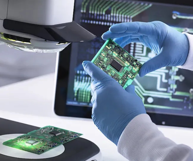
09.Electrical Testing & Final Inspection
Every board undergoes electrical continuity and isolation testing to verify open/short circuits. Visual inspections and AOI (Automated Optical Inspection) ensure trace accuracy and pad quality. Additional tests may include X-ray, dimensional checks, and bend-cycle reliability tests.
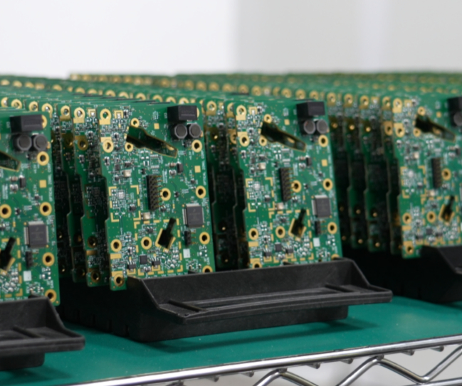
10.Final Cutting, Packaging & Shipping
Finished PCBs are laser-cut or routed into final shape and packaged in ESD-safe materials. Custom labeling, serialization, and documentation are included per customer request.
Why It Matters?
Each stage in Flex PCB manufacturing directly impacts functionality, reliability, and cost. With our IPC-compliant processes, experienced technicians, and in-house DFM engineering, we ensure your designs are built right — from prototype to production.
Industry Applications for Flex PCBs
Flexible printed circuit boards are essential in industries where space constraints, weight reduction, and mechanical flexibility are critical. Our Flex PCBs are widely adopted across the following sectors:


FAQ
The recommended minimum bend radius depends on whether the flex area is static or dynamic:
- Static Flexing: Minimum radius = 6× the board thickness
- Dynamic Flexing: Minimum radius = 12× or more of the board thickness
Using rolled annealed (RA) copper improves bendability and extends flex life.
Flex PCBs are primarily made from polyimide (PI) or polyester (PET) substrates with copper foil layers. We also use adhesiveless laminates for high-reliability applications. Coverlays, stiffeners (FR4 or stainless steel), and surface finishes (ENIG, OSP) are added depending on the design.
Lead times depend on complexity and quantity:
- Prototype Flex PCBs: 3–7 business days
- Production Runs: 7–20 business days
Expedited options are available for urgent projects — contact us for a custom quote.
Yes. We offer full Rigid-Flex PCB manufacturing, including HDI and multilayer designs. Our process supports complex 3D assemblies and ensures precise layer registration and bend reliability.
We offer a range of surface finishes to meet different electrical and soldering requirements:
- ENIG (Electroless Nickel Immersion Gold) – best for fine-pitch and wire bonding
- OSP (Organic Solderability Preservative) – cost-effective, RoHS compliant
- Immersion Silver / Tin, Lead-Free HASL, and others available upon request
- Flex PCBs use flexible base materials and are designed to bend, fold, or twist during use.
- Rigid PCBs are built on FR4 substrates and are not designed for movement.
Flex PCBs save space, reduce weight, and improve durability in dynamic environments.
Absolutely. Our engineering team offers free DFM reviews, helping you optimize your design for manufacturability, cost efficiency, and long-term reliability. Upload your Gerber files, and we’ll evaluate them before production begins.
Yes. All our Flex PCBs are RoHS-compliant and manufactured to IPC-6013 and IPC-A-600/610 Class 2 or Class 3 standards, depending on application needs. Certifications and test reports are available upon request.
To provide an accurate and fast quote, please include:
- Gerber files (RS-274X format preferred)
- Bill of Materials (BOM) if assembly is needed
- Stack-up or layer information
- Quantities and delivery timeline
- Special requirements (e.g., stiffeners, impedance control, finish type)