Maintain signal integrity in high-speed and RF designs with precision-controlled impedance PCBs. With stackup-driven engineering, tight process control, and impedance coupon/TDR verification options, we deliver repeatable results from fast-turn prototypes to production.
Controlled impedance PCBs are essential for high-speed digital and RF designs where signal integrity can’t be left to chance. When impedance drifts outside the target, you can see reflections, eye-diagram collapse, timing errors, and EMI issues—especially on long runs, dense multilayer boards, and high-speed interfaces.
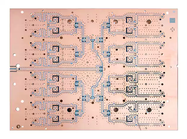
FastTurn builds controlled impedance PCBs for applications such as high-speed interfaces, RF/microwave designs, and high-density multilayer layouts. Our process starts with stackup-driven engineering and continues with fabrication controls that maintain consistent critical geometry, helping you achieve repeatable electrical performance across builds.
Whether you’re ordering prototype quantities, high-mix low-volume builds, or small-to-medium production runs, we support a smooth transition from validation to scalable manufacturing. Controlled impedance fabrication can be integrated with multilayer PCB builds, and—when required—special materials and advanced processes under a unified fabrication workflow.
What Is a Impedance Control PCB ?
A controlled-impedance PCB is a printed circuit board designed and manufactured so that its transmission lines maintain a specific characteristic impedance. This is achieved by controlling the relationship between trace geometry (width/spacing), dielectric thickness, and reference planes in the stackup.
Impedance can be specified for single-ended traces or differential pairs, and your design rules and interface requirements typically define it. Common target values in industry include 50Ω, 90Ω, and 100Ω (examples only—your design may differ).
Controlled impedance is most critical in high-speed, high-frequency circuits where traces behave like transmission lines and electrical performance depends on consistent impedance from build to build.
Why Impedance Control Matters?
Impedance control directly impacts signal integrity and system stability. When impedance is not managed, signals can reflect from discontinuities, distorting the waveform, reducing the noise margin, and increasing bit errors. On high-speed links, even slight variations can affect timing, crosstalk, and EMI.
Key benefits of controlled impedance PCBs
Reduces reflections and waveform distortion
Improves eye openings and timing margins on high-speed interfaces
Helps manage crosstalk and supports cleaner differential signaling
Improves EMI/EMC performance by stabilizing transmission behavior
Supports compliance with interface and system-level requirements
For designs that must pass validation quickly and scale reliably, controlled impedance manufacturing is a practical way to reduce risk before prototypes become production programs.
Impedance Structures & Types
Controlled impedance can be implemented using different transmission line structures depending on the routing layer, stackup, and performance goals.
Microstrip
Outer-layer trace referenced to an internal plane. Ordinary for routing that requires easier access or shorter return paths, with solder mask effects considered.
Stripline
Inner-layer trace sandwiched between planes. Often preferred for tighter control, better shielding, and reduced EMI—commonly used for critical high-speed nets.
Differential Microstrip
Outer-layer differential pair. Useful for fast routing and connector transitions, with tight spacing control to maintain differential impedance.
Differential Stripline
Inner-layer differential pair. Often used for the most demanding high-speed differential links due to its stable geometry and shielding.
Key Factors That Affect Impedance
Controlled impedance depends on the stackup and the manufacturing window. The most critical contributors include:
Solder mask & process variation: outer-layer mask thickness can shift impedance on microstrips
Discontinuities: via transitions, plane breaks, connector launches, neck-downs, stubs
Because these factors interact, the best results come from aligning your impedance targets with a manufacturable stackup and controlled process parameters early in the cycle.
Impedance Control Capabilities
FastTurn supports controlled impedance fabrication across a wide range of board types, from prototypes to production programs, with stackup-based engineering and process controls designed for repeatability.
Tolerance Options
Many projects target ±10% impedance tolerance, with ±5% often requested for tighter designs. Final tolerance capability depends on stackup, geometry, materials, and verification method, and is confirmed during engineering review.
Controlled impedance is commonly implemented in multilayer stackups for better shielding and stability. We support multilayer builds where impedance targets must remain consistent across layers and production lots.
RF / High-Speed Material Support
When projects require enhanced high-speed or RF performance, material selection becomes part of impedance success. We can review targets and recommend manufacturable stackup approaches aligned with your performance goals.
Quality & Certifications
FastTurn PCBs maintains strict quality, safety, and compliance standards across all controlled impedance PCB manufacturing programs. Our quality system is reinforced by engineering reviews, in-process inspections, and verification options that support repeatable impedance performance from prototypes to production. Quality control is embedded throughout our PCB fabrication workflow—from incoming materials and stackup planning to final electrical test and shipment.
Quality at Every Step
Each impedance-controlled PCB build follows documented controls to support signal integrity, stackup consistency, and manufacturing repeatability.
Stackup & Impedance Engineering Review
Front-end review of impedance targets, controlled layers, and build intent to align geometry with a manufacturable stackup.
Process Control for Trace Geometry
Etch compensation and manufacturing controls to help maintain consistent trace width/spacing that impacts impedance.
Material & Lamination Consistency
Controlled handling of core/prepreg and lamination parameters to support stable dielectric thickness and board-to-board consistency.
Inspection & Electrical Testing
In-process inspections and final electrical testing to detect opens/shorts and verify fabrication integrity before assembly.
Impedance Verification Options
When required, impedance test coupons and TDR-based measurement/reporting can be supported in accordance with your documentation and verification plan.
Certifications
FastTurn PCBs follows internationally recognized quality and compliance practices to support high-reliability PCB fabrication.
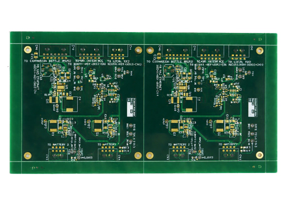
Our portfolio includes controlled-impedance PCBs designed for high-speed digital and RF applications. Each build reflects our focus on stackup accuracy, repeatable trace geometry, and consistent impedance results from prototype to production.
Prototyping to Production
FastTurn supports controlled impedance PCBs from fast-turn prototypes to repeatable production. We focus on stackup consistency, documented build intent, and process stability so your validated prototype can scale without unexpected electrical shifts.
Our prototype-to-production workflow supports
NPI programs and rapid validation cycles
Fast engineering feedback on manufacturability and stackup alignment
High-mix builds with controlled documentation.
Stable manufacturing windows for small-to-medium production runs.
Smoother transitions with fewer redesigns and fewer surprises
Industries & Applications We Support
We serve a diverse range of industries with precision-built controlled impedance PCBs, engineered to meet application-specific requirements for signal integrity, high-speed performance, and repeatable electrical reliability.
FastTurn PCBs provides controlled-impedance PCB manufacturing for industries that require dependable signal integrity, stable high-speed performance, and repeatable electrical performance. Our capabilities support both high-speed digital and RF designs where impedance consistency is essential for meeting interface requirements and reducing EMI risk. Through stackup-driven engineering and controlled fabrication processes, we deliver impedance-controlled PCBs aligned with application-specific technical needs.
Industries & Applications
Aerospace & Defense
Medical & Life Sciences
Industrial & Automation
Communications
Data & Computing
Energy & Power Systems
Why FastTurn PCB?
FastTurn PCBs delivers controlled impedance PCB solutions built on engineering alignment, process discipline, and scalable manufacturing support. From fast-turn prototypes to repeatable production runs, we help customers meet impedance targets with fewer iterations and more predictable electrical performance.
Diverse Industry Expertise
We support industrial, medical, energy, communications, and other high-reliability industries, delivering through-hole PCB assembly and mixed-technology PCBA for applications with demanding mechanical and environmental requirements.
End-to-End PCB Assembly Solutions
FastTurn provides end-to-end PCB assembly services under one controlled workflow. Early DFM involvement helps reduce risk and enables a smooth transition from fast-turn prototypes to scalable production.
Turnkey Assembly Services
Our turnkey PCB assembly services include component sourcing, SMT and through-hole assembly, testing, and final integration—simplifying supply chains and improving execution consistency.
Advanced Manufacturing Capabilities
We support complex PCB assemblies through controlled processes, skilled technicians, and flexible assembly lines suited for high-mix and low-to-medium volume production.
Comprehensive Testing & Quality Control
Quality is embedded throughout our PCB assembly process, with inspection and testing methods applied to detect issues early and ensure long-term reliability.
Efficient Lead Times
Streamlined workflows and responsive engineering enable fast prototype turnaround and reliable production schedules without compromising assembly quality.
Inside Our Facilities
Our facilities are equipped to support controlled impedance PCB fabrication, with manufacturing workflows built around stackup consistency, trace-geometry control, and final electrical verification. From engineering review and process documentation to inspection and electrical testing, we maintain a disciplined build approach designed to deliver repeatable impedance performance across prototypes and production programs.
FAQ
What is a controlled impedance PCB?
A controlled-impedance PCB is manufactured so that critical traces maintain a defined characteristic impedance (single-ended or differential) based on stackup geometry and controlled fabrication processes.
When do I need impedance control?
Impedance control is typically needed for high-speed digital links and RF sections where signal integrity and EMI performance are critical.
What’s the difference between single-ended and differential impedance?
Single-ended impedance applies to one trace referenced to a plane. Differential impedance applies to a matched pair whose spacing and geometry define the pair’s behavior together.
What do you need to quote an impedance-controlled PCB?
Gerbers/ODB++, layer count/stackup (or constraints), an impedance table (targets), tolerance (if specified), and identification of critical nets/layers.
Do you provide impedance coupons and TDR reports?
Coupons and TDR verification can be supported when required, based on your verification plan and documentation needs.
What tolerance can you hold for impedance control?
Many projects use ±10%, and tighter targets such as ±5% may be achievable depending on stackup, materials, geometry, and verification requirements.
Looking for an expert quick-turn to turnkey PCB solution?
FastTurn PCB specializes in higher layer count PCBs, quick-turn manufacturing, HDI structures, blind and buried vias, as well as controlled impedance and precision fabrication processes.