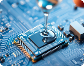
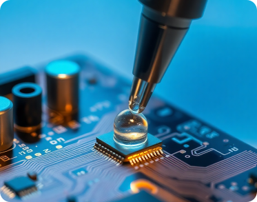
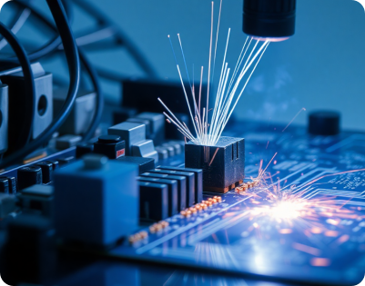
Controlled Reflow Soldering Processes: Professional temperature profiling ensures superior solder joint quality and reliability.
ESD & Temperature-Controlled Environment: All assembly processes are carried out in strictly controlled anti-static, temperature and humidity environments, safeguarding your sensitive electronic components.
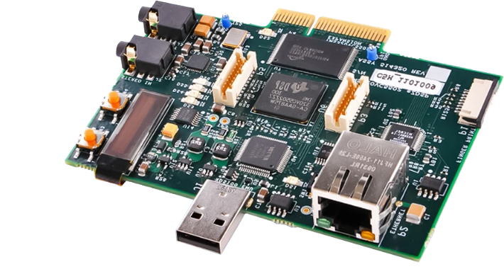
Rework & Reballing Services
Solder joint repair and component replacement for BGA chips.
Precise solder ball reattachment (reballing), accurately restoring original solder layouts.
PCB pad repair and cleaning, extending the lifespan of your circuit boards.
We implement rigorous quality management practices from raw material inspection through final product delivery, ensuring the reliability and stability of every solder joint.
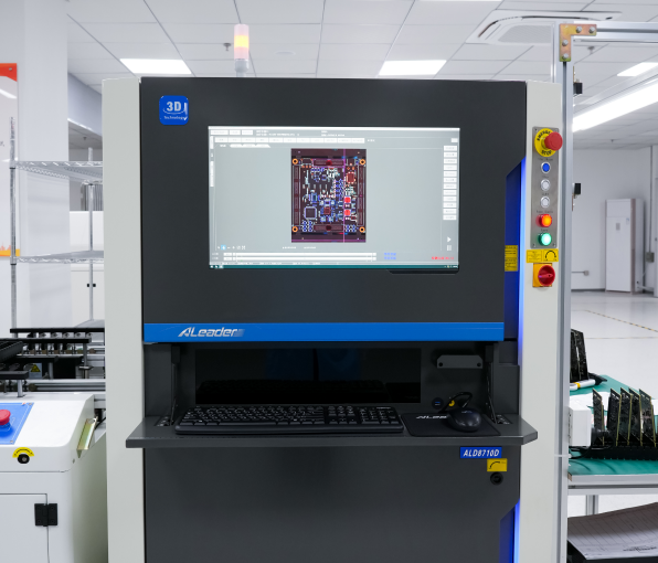
Step 1
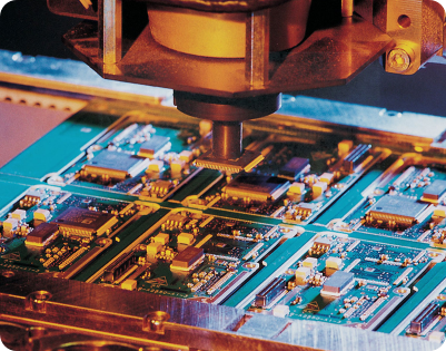
Automated Optical Inspection (AOI)
We utilize state-of-the-art Automated Optical Inspection (AOI) systems with high-precision visual recognition technology to swiftly identify placement deviations, solder defects, and solder joint quality issues, significantly reducing potential failure risks.
Rapid and accurate detection of component misplacement and missing components.
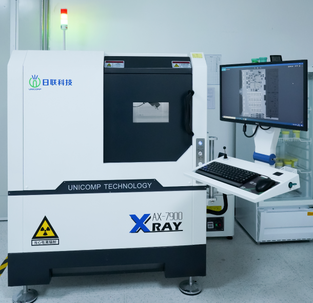
Since BGA solder joints are hidden beneath components, we employ high-resolution X-ray non-destructive inspection equipment to visually assess solder joint internal structures, ensuring joints are free of voids, cracks, or inadequate soldering.
Precise identification of minute internal defects within solder balls.
Detailed X-ray inspection reports provided to customers, ensuring transparent and traceable production.
Step 3
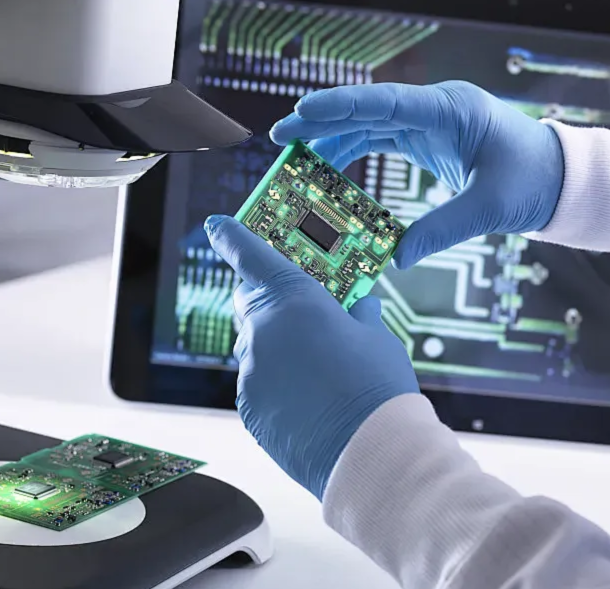
Design for Manufacturability (DFM) Review
To ensure smooth production of your project, our professional engineering team provides comprehensive Design for Manufacturability (DFM) reviews, covering pad dimensions, solder-mask openings, and soldering process optimization, effectively reducing design flaws and minimizing production risks.
Expert guidance on optimal BGA pad designs, recommending ENIG finishes and NSMD pads.
Reduced production costs and increased first-pass yield rates.
Step 4
Strict Production Standards & Certification System
We strictly adhere to international standards such as IPC-A-610 and ISO9001 in our production and inspection processes, ensuring every BGA assembly step meets regulatory requirements and client specifications.
Compliance with IPC-A-610 Class II and III standards (commercial and military-grade).
ISO9001 Quality Management System certified, continuously guaranteeing consistent quality.
Industry Application
We understand each industry’s unique requirements and are ready to tackle your most complex technical challenges.
Chosen by 9000+ Customers– Your Satisfaction Drives Us Forward.
FastTurn PCB delivers consistent manufacturing quality, fast responses, and dependable delivery for prototypes and mass production. Engineers and OEM teams worldwide rely on us to keep their projects moving smoothly and on schedule.
Les Komarck
US
Great prices, lead times, and quality of work
Great news.Well done,it was fast turn indeed.Your ability to maintain such high standards while delivering ahead of schedule is greatly appreciated. This timely completion has already made a positive impact,Many thanks again for your excellent work.Let's schedule a call next week to discuss the next phase.
DATE OF experience:
July 21,2025
Gio
CA
Completely satisfied with your service and PCBs.
I'm truly delighted with the PCB manufacturing service provided by your company! I checked the PCBs in my design,all specifications meet my requirements perfectly,
I'm completely satisfied with your service and PCBs.
I rate your products and services a perfect 5/5 stars. Thank you for helping bring my electronic designs to life!
DATE OF experience:
May 1, 2024
Edwin
UK
Good package with service, price, quality and delivery time.
Tracking number received, Fastturn do a good job!
In the moment I see a good package with service, price, quality and delivery time at
Fastturn, Excels in packaging craftsmanship, service professionalism, cost-effectiveness, product quality, and punctual delivery.Hopefully this will last the next years. Regards.
DATE OF experience:
Apr 07, 2023
Glenn
US
Reliable company, outstanding in precision work.
This is tremendous news! Many thanks to you and your team for your dedication and hard work - it's very impressive. I genuinely appreciate your tireless efforts to help us achieve our goals, continuing our productive partnership in future endeavors. Warmest regards and sincere appreciation for making this achievement possible.
DATE OF experience:
Dec 13, 2024
Duy Nguyen
ISR
We are quire satisfy with your services,thanks.
We received your PCB shipped from Fastturn.We are satisfied with your services. There are no issues with delivery time, circuit board appearance, or packaging.Our team are doing some extra test before making conclusion.Anyway, thank so much for your effort to support us,looking forward to next collaboration. Best regards.
DATE OF experience:
Mar 02, 2024
Adrian Gal
SG
We will recommend your company definitely to others.
A pleasant collaboration can be given a score of five
communication: 5 out of 5. Very good communication skills,
leading time: 5 out of 5. The manufacturing time of the PCBs
quality: 5 out of 5. PCB and PCBA quality meets our requirements.
Overall process: 5 out of 5.We will recommend your company definitely to others.
DATE OF experience:
Nov 09, 2024
Iorio
US
Well produced,Quick turn,well packaged,fast shipping.
The products are great, really well-made! The whole buying process was smooth and professional, especially how quickly they handled the order. From start to finish, everything worked perfectly—they even packed everything super carefully. You can tell the seller really cares about the details!"
DATE OF experience:
Jul 26, 2024
MarcBoers
US
Received your parts today,they look very good.
Thank you for the expedited shipment - received prototype parts today in perfect condition. Initial inspection appears satisfactory, Your team's remark able speed in both production execution and competitive pricing for this trial order has been impressive. Looking forward to volume production discussions pending test outcomes.
DATE OF experience:
Sept 29, 2024
FAQ
Q:What types of BGA packages can you handle?
Q:What types of BGA packages can you handle?
Q:What's the smallest BGA pitch you can reliably assemble?
Our equipment supports precision BGA assembly down to a minimum pitch of 0.25 mm.
Q:Do you provide BGA reballing and rework services?
Yes, we offer professional BGA reballing and rework services, including solder ball replacement, solder joint repair, and PCB pad refurbishment.
Q:How do you ensure the quality of solder joints in hidden areas under the BGA?
We employ advanced X-ray inspection equipment to visualize and ensure the integrity of solder joints beneath BGA chips.
Q:What's your typical turnaround time for BGA assembly projects?
Standard projects typically complete within 5-7 days. Quick-turn prototypes can be finished in as little as 24 hours, depending on complexity.
Q:Can you handle small-volume prototype orders?
Absolutely! We specialize in prototype and low-volume orders and offer customized solutions for rapid prototyping.
Q:Do you provide DFM (Design for Manufacturability) reviews?
Yes, our engineers offer comprehensive DFM reviews to optimize your PCB layout, pad design, and solder mask for the best production results.
Q:What certifications and standards do your services comply with?
Our processes strictly follow IPC-A-610 Class II and III standards and are ISO9001 certified, ensuring consistent high quality.
Q:Do you support special surface finishes like ENIG for BGA pads?
Yes, we recommend and frequently utilize ENIG finishes with NSMD pads for optimal solderability and reliability.
Q:Can you provide inspection reports and documentation for quality assurance?
Of course! We provide detailed AOI and X-ray inspection reports with every project to ensure complete transparency and traceability.