PCB Fabrication Low Cost Guide 2026: Save Without Sacrificing Quality
PCB fabrication low cost guide: smart choices on materials, thickness, finish, testing & lead time, plus 2026 supplier rankings—affordable boards without risk.
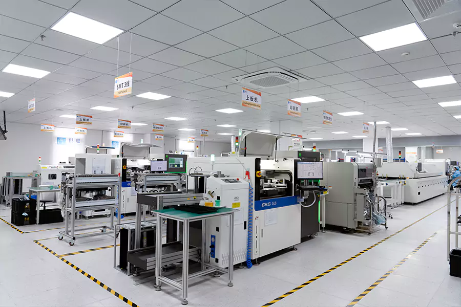
Quick Turn PCB & Assembly in the USA – 24–72 Hour Prototypes Done Right
Learn how to get reliable quick turn PCB and PCB assembly in the USA — 24–72 hour prototypes, turnkey options, practical DFM tips, and how to cut lead time without risking quality.
PCB Surface Finish: ENIG vs HASL vs OSP & More — Which Is Best for Your Board?
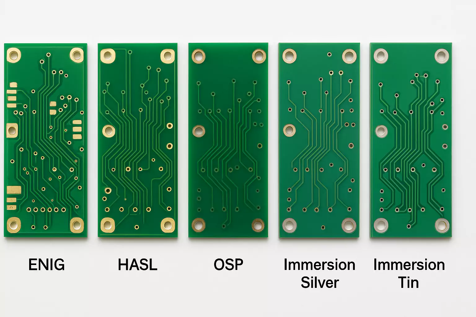
Compare the most common PCB surface finishes—ENIG, HASL, OSP, Immersion Silver, and Immersion Tin. Learn how each affects solderability, cost, reliability, and RoHS compliance to choose the best finish for your PCB design
PCB Panelization Guide: Best Practices for Efficient Layout, V-Scoring, and Tab Routing
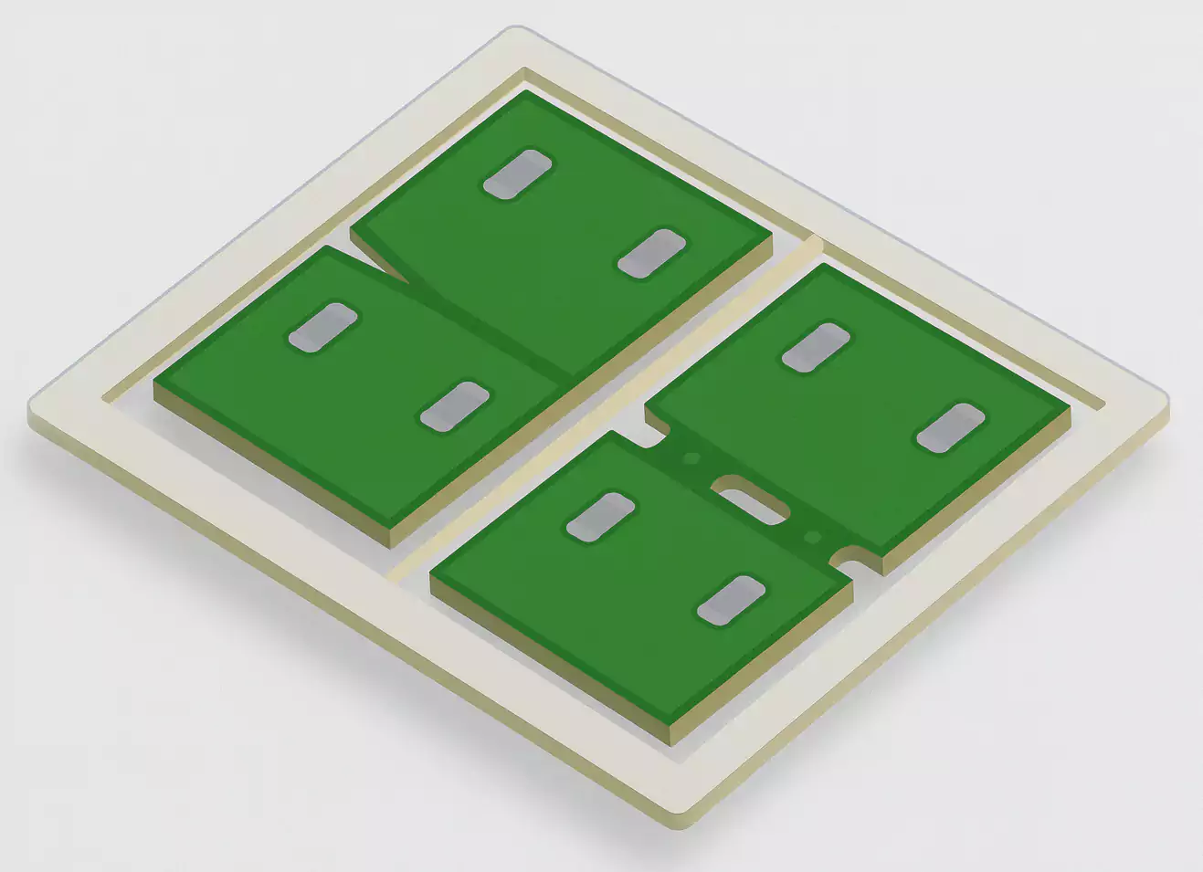
Learn everything you need to know about PCB Panelization—from V-scoring vs. tab-routing to array layout, fiducial placement, and edge rail design.
Solder Mask and Silkscreen Process
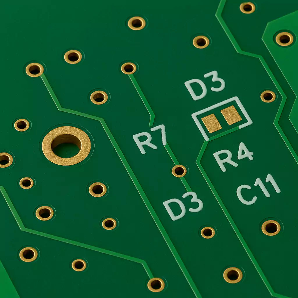
Discover how solder mask and silkscreen layers impact PCB reliability. This guide covers essential process steps, design best practices, and how to prevent common issues like pad misalignment and silkscreen overlap.
PCB Drilling and Plated Through Holes
Learn everything about PCB drilling and plated-through holes—including drilling methods, plating processes, quality factors, common defects, and DFM guidelines to avoid manufacturing issues.
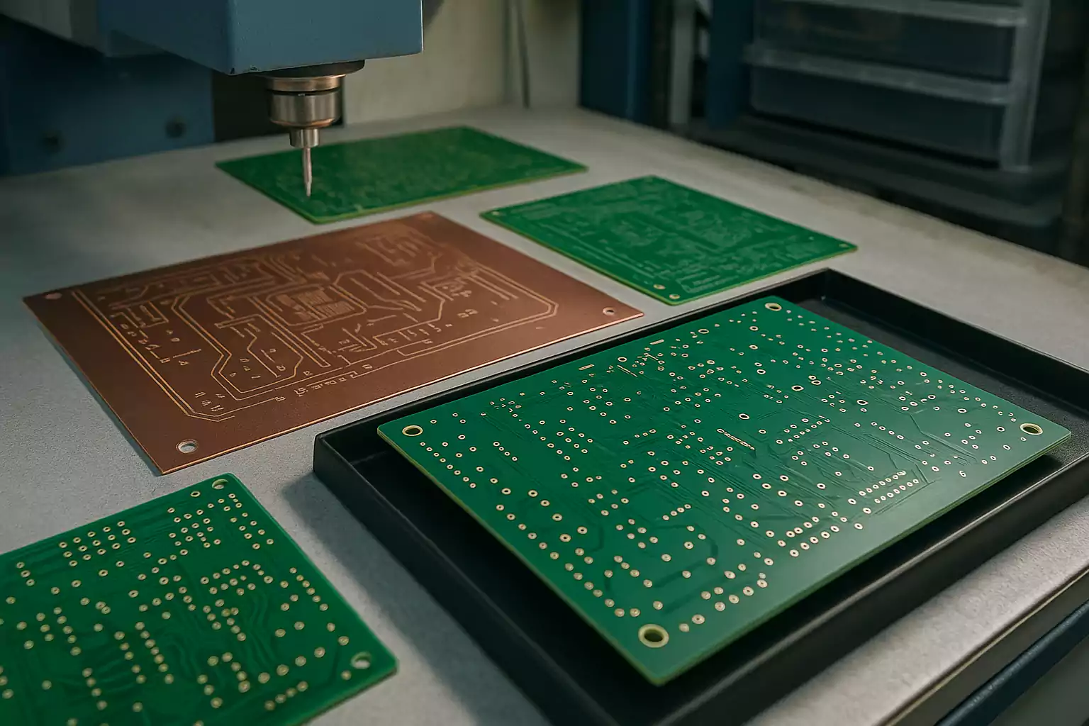
Inner Layer Imaging and Lamination
Learn how inner layer imaging and lamination shape the quality and reliability of multilayer PCBs. This expert guide covers photoresist patterning, etching, material shrinkage, stack-up design, and process control—essential for engineers optimizing multilayer board performance.
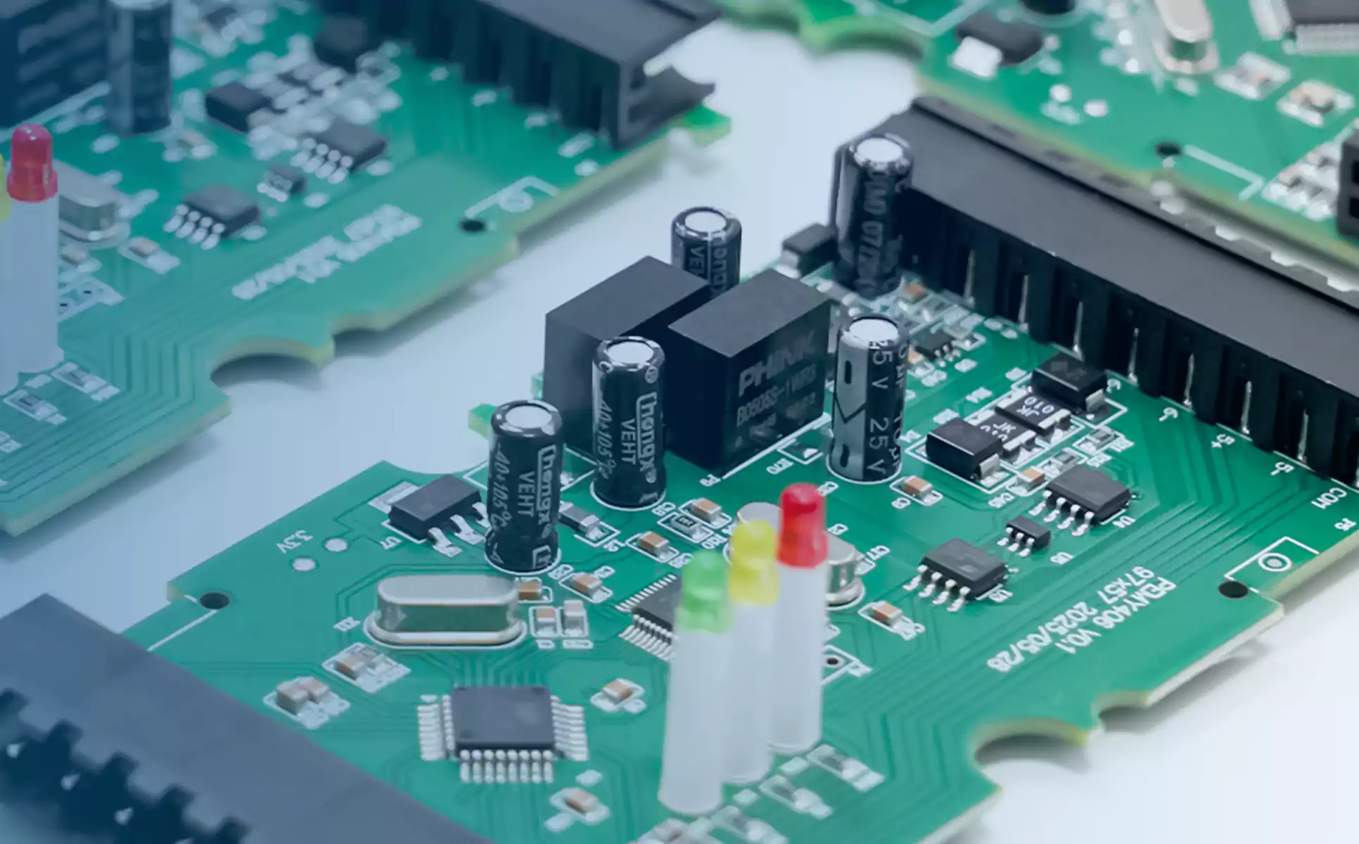
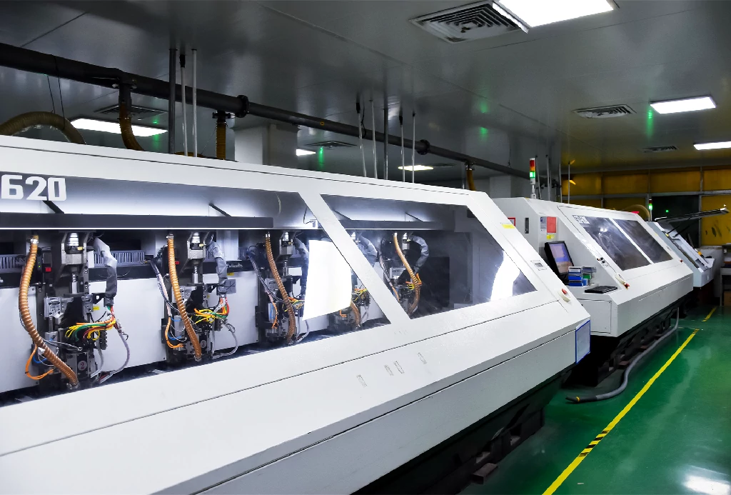
Full Overview of PCB Manufacturing Process
Explore the complete PCB manufacturing process—from design files to finished boards. Learn every key step including imaging, drilling, plating, solder mask, and testing. Ideal for engineers and teams seeking reliable, high-quality PCB production.