Introduction: What is SMT (Surface Mount Technology)?
Surface Mount Technology (SMT) is a method of mounting electronic components directly onto the surface of printed circuit boards (PCBs). Unlike traditional through-hole technology (THT), SMT components are placed on the surface, allowing for smaller, more efficient designs and faster production times.
SMT has become essential in the manufacturing of modern electronics, from smartphones to automotive systems. Its ability to support high-density, high-performance devices makes it the preferred choice for mass production.
In this guide, we’ll cover the basics of SMT, its key process steps, and best practices for achieving high-quality results.
A Brief History of SMT: From Innovation to Industry Standard
Surface Mount Technology (SMT) has become the backbone of modern electronics manufacturing, but its origins trace back several decades. Understanding the evolution of SMT provides valuable insight into how electronic assembly has advanced from bulky, manual processes to today’s high-speed, high-precision, and highly automated systems.
The Emergence of SMT in the 1960s–1970s
Prior to the advent of SMT, Through-Hole Technology (THT) dominated electronic assembly. Components were inserted into pre-drilled holes on printed circuit boards (PCBs) and soldered manually or via wave soldering. While reliable, this method limited component density, increased production time, and constrained miniaturization.
In the late 1960s to early 1970s, driven by the need for smaller, lighter, and more cost-effective consumer electronics, engineers began experimenting with mounting components directly onto the PCB surface. This new method eliminated the need for holes, reduced board space requirements, and allowed for both sides of the PCB to be populated—marking the birth of Surface Mount Technology.
Growth in the 1980s: From R&D to Mass Production
By the 1980s, SMT was no longer just an experimental idea. Major electronics manufacturers in Japan and the U.S. had begun integrating SMT into mass production. This period saw the introduction of:
- SMDs (Surface-Mount Devices) like chip resistors, capacitors, and transistors
- Pick-and-place machines for automated component placement
- Reflow soldering as a standard thermal process for solder joint formation
The ability to increase component density while reducing board size and manufacturing costs made SMT the preferred solution for emerging technologies like personal computers, mobile phones, and industrial controllers.
Standardization and Global Adoption in the 1990s
As SMT matured, industry standards were established by organizations such as IPC, JEDEC, and IEC to regulate footprint designs, solderability, component packaging, and inspection guidelines. These efforts helped ensure cross-vendor compatibility and improved manufacturing yield.
By the mid-1990s, SMT had become the de facto standard for PCB assembly across industries—from consumer electronics to aerospace. Even traditional THT was often used only for connectors or components that required high mechanical strength.
2000s–Now: Advancements in Miniaturization and Automation
The 21st century brought unprecedented advancements in miniaturization, automation, and process control. Notable developments included:
- Ultra-fine pitch components (e.g., 0.3mm QFNs and BGAs)
- Advanced placement machines with sub-30-micron accuracy
- Automated Optical Inspection (AOI) and X-ray systems for real-time defect detection
- No-clean fluxes and lead-free soldering to meet environmental regulations
Today, SMT supports cutting-edge applications like 5G infrastructure, IoT devices, wearable technology, and electric vehicles. The technology continues to evolve with the integration of machine learning, closed-loop feedback systems, and smart factory platforms.
Key Milestones in SMT Development
| Year | Milestone |
|---|---|
| Late 1960s | First surface-mount concepts introduced in aerospace and defense sectors |
| 1970s | Prototype SMDs developed and tested in low-volume applications |
| 1980s | Commercial adoption begins; reflow ovens and placement machines developed |
| 1990s | Standardization by IPC and global mass adoption |
| 2000s | Emergence of fine-pitch components and lead-free soldering |
| 2010s–Now | AI-driven SMT lines, smart factories, and 01005-sized SMDs |
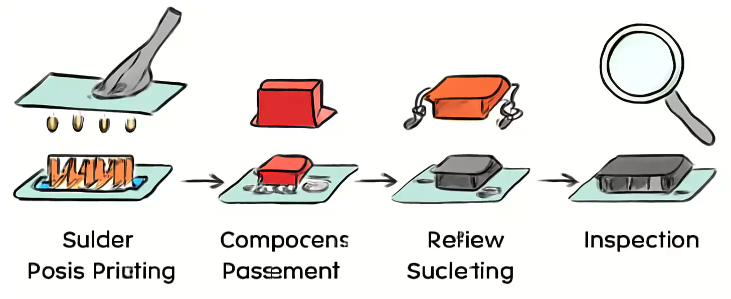
Core SMT Process Flow
Surface Mount Technology (SMT) is a highly efficient assembly process for placing electronic components onto printed circuit boards (PCBs). The process involves several key stages, each crucial for ensuring the quality and reliability of the final product. Below is a step-by-step overview of the typical SMT process flow.
1. PCB Design and Preparation
Before the assembly process begins, the PCB must be designed with SMT-specific requirements in mind. Key considerations include:
- Land Pattern Design: Ensuring the PCB pads align with component leads for proper soldering.
- Solder Mask Openings: Accurate design to avoid solder bridging or inadequate solder coverage.
- Panelization: Multiple boards are grouped into panels to streamline the manufacturing process.
The design phase sets the foundation for the rest of the assembly process, so applying Design for Manufacturability (DFM) principles early is critical to avoid downstream issues.
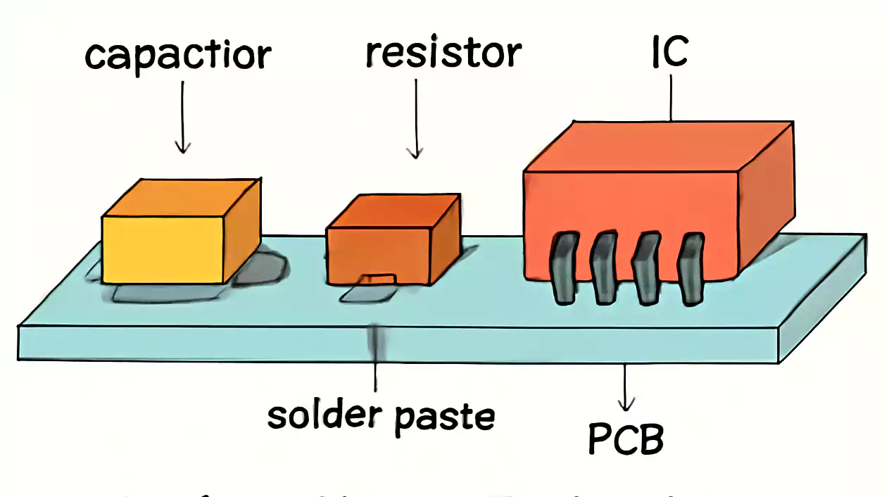
2. Solder Paste Printing
Solder paste printing is the first physical step in the SMT process, where solder paste is applied to the PCB pads.
- Stencil: A metal stencil is used to apply a precise amount of solder paste to each pad.
- Printing Process: The solder paste is deposited through the stencil, and a squeegee ensures uniform coverage.
The quality of this step is critical, as insufficient or excessive paste can lead to defects. Solder Paste Inspection (SPI) is often used to verify the amount and placement of paste on each pad.
3. Component Placement
In this step, electronic components are placed onto the PCB using automated pick-and-place machines. These machines are capable of placing thousands of components per hour with high precision.
- Feeding Systems: Components are fed to the machine from reels or trays.
- Placement: The machine's vision system aligns each component with its corresponding pad.
Precision is key here, as misalignment or component misplacement can lead to costly defects such as solder bridges or tombstoning.
4. Reflow Soldering
Once the components are placed on the board, the assembly moves to the reflow oven, where the solder paste is melted to create solid solder joints.
- Preheat: The board is gradually heated to activate the flux in the solder paste.
- Reflow: The temperature reaches its peak, allowing the solder to melt and form a bond between the component leads and the pads.
- Cooling: The board is cooled rapidly to solidify the solder joints.
The temperature profile is carefully controlled to avoid issues such as cold solder joints or excessive heating that could damage components.
5. Inspection and Quality Control
After reflow soldering, thorough inspection is necessary to ensure the quality of the assembly. Common inspection methods include:
- Automated Optical Inspection (AOI): Detects visual defects like misalignment, solder bridges, and missing components.
- X-ray Inspection: Used for more advanced components like BGAs (Ball Grid Arrays) that are not visible to AOI systems.
- In-Circuit Testing (ICT): Verifies that all electrical connections are intact.
These methods help identify and address defects before the final product leaves the production line.
6. Rework and Repair
Not all defects require scrapping; many can be corrected with rework:
- Hot Air Rework: Used for components that need to be desoldered and replaced.
- Manual Touch-Up: For small, localized defects, such as insufficient solder or misalignment.
Rework can be time-consuming, so it’s important to minimize defects during the initial assembly stages through process control.
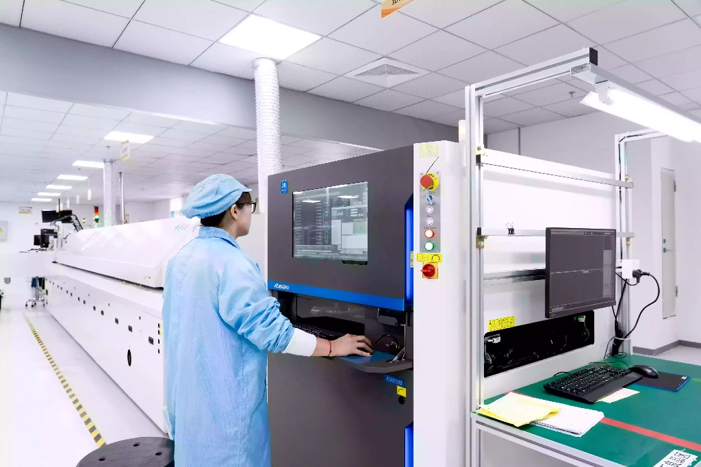
SMT Equipment Selection Guide
Selecting the right SMT (Surface Mount Technology) equipment is essential for achieving high-quality, reliable, and efficient electronics manufacturing. This guide walks you through the core equipment types used in SMT assembly, key factors to consider when choosing equipment, and tips for selecting the right tools based on production needs.
1. Key SMT Equipment Types
The following core machines are essential in any SMT production line:
- Stencil Printer: Used for applying solder paste to the PCB’s pads using a stencil and squeegee mechanism.
- Pick-and-Place Machine: Accurately places surface-mount components onto soldered PCB pads.
- Reflow Oven: Melts solder paste to create permanent connections between components and PCB.
- Inspection Equipment: Ensures the quality of the assembly by detecting defects like misalignment or poor solder joints.
- Conveyor Systems: Used to move PCBs through the production line efficiently.
2. Stencil Printer: Precision Matters
A stencil printer is used to apply solder paste onto the PCB. Accurate paste deposition is critical for ensuring proper solder joints during reflow soldering.
Considerations when selecting a stencil printer:
- Print accuracy: Choose a machine that ensures tight tolerances, especially for small components like 0201 or 0402.
- Stencil cleaning system: Automatic cleaning helps reduce downtime.
- Solder paste inspection (SPI): Some printers come with built-in SPI systems for real-time monitoring of paste deposition quality.
3. Pick-and-Place Machine: Speed vs. Precision
The pick-and-place machine is at the heart of an SMT line. It places components onto the PCB after solder paste has been applied.
Factors to consider:
- Placement accuracy: Ensures components are positioned correctly to avoid misalignment.
- Speed: The machine should be fast enough to meet production targets but not sacrifice precision.
- Component size range: Ensure the machine can handle the range of components your production requires (from large components like connectors to small ones like 0201 chips).
4. Reflow Oven: Ensuring Reliable Solder Joints
The reflow oven is used to heat the PCB and solder paste to form reliable solder joints. A properly configured reflow profile is essential to prevent defects such as cold solder joints or voids.
Key features to look for:
- Heating zones: A higher number of heating zones allows for more precise temperature control.
- Temperature profiling: It’s crucial to monitor the solder paste’s melting point and avoid overheating components.
- Nitrogen capability: Nitrogen is often used to reduce oxidation during the reflow process, especially for lead-free soldering.
5. Inspection Systems: Quality Control
Inspection is vital in SMT to ensure high-quality assembly. Common inspection systems include:
- SPI (Solder Paste Inspection): Verifies paste volume and coverage before component placement.
- AOI (Automated Optical Inspection): Checks for misalignment, solder defects, and component placement errors post-placement.
- X-ray Inspection (AXI): Used for inspecting hidden solder joints, such as those in BGAs (Ball Grid Arrays).
Why inspection matters:
- Early defect detection: Catching issues early in the process minimizes waste and rework.
- Quality assurance: Helps maintain consistent production quality and reduce the risk of failure in the final product.
6. Support Equipment: Enhancing Production Efficiency
To ensure smooth operation, several support systems can complement the core SMT equipment:
- Conveyors: Used to transport PCBs through different machines, increasing production efficiency.
- Moisture-sensitive component storage: Essential for preventing damage to components that are sensitive to moisture (e.g., BGAs).
- Drying ovens: Used for components that require moisture removal before soldering.
Additional automation: Consider integrating with Manufacturing Execution Systems (MES) for real-time monitoring and production management.
7. How to Choose the Right Equipment
Selecting the appropriate SMT equipment depends on your production scale and product complexity.
- For low-volume production: A semi-automatic stencil printer and a desktop pick-and-place machine may suffice.
- For medium-volume production: A fully automated stencil printer, pick-and-place machine, and reflow oven with 8 zones are recommended.
- For high-volume production: Consider investing in high-speed, multi-head pick-and-place machines, advanced reflow ovens with nitrogen capability, and inline SPI/AOI systems for quality control.
SMT vs THT vs Mixed Assembly: Key Differences
When choosing the right assembly method for a PCB, Surface Mount Technology (SMT), Through-Hole Technology (THT), and Mixed Assembly each offer distinct advantages depending on the application and production needs.
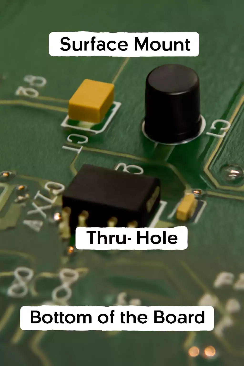
What is SMT (Surface Mount Technology)?
SMT is a method where electronic components are mounted directly onto the surface of the PCB. The components used are typically smaller and lighter, designed to be placed onto pads on the PCB’s surface without requiring holes.
Advantages of SMT:
- High Density: Ideal for compact, high-performance devices.
- Faster Assembly: Automated pick-and-place machines can quickly place components, making it cost-effective for large-scale production.
- Better Electrical Performance: Shorter lead lengths reduce signal distortion.
Limitations:
- Rework Complexity: Manual soldering and rework are difficult, especially for small components like QFNs or BGAs.
- Mechanical Stress: Not suitable for components that will face high mechanical stress, such as connectors or large capacitors.
What is THT (Through-Hole Technology)?
THT involves inserting components with leads through holes in the PCB and soldering them on the other side. It has been used for decades and remains popular for applications requiring strong mechanical bonds.
Advantages of THT:
- Strong Mechanical Bond: Provides a more robust connection, making it ideal for heavy or high-stress components.
- Easier Rework: Manual soldering and rework are easier compared to SMT, especially for prototype builds.
- Reliable in Harsh Environments: Often used for high-reliability applications like aerospace and automotive.
Limitations:
- Lower Density: THT requires larger boards and spaces between components.
- Slower Assembly: More manual handling and time-consuming than SMT.
What is Mixed Assembly?
Mixed Assembly combines both SMT and THT techniques on the same PCB. This method is used when certain components, such as large connectors, need the mechanical stability of THT, while the rest of the board benefits from SMT’s high density and efficiency.
Advantages of Mixed Assembly:
- Flexibility: It allows for both high-density components (SMT) and components requiring strong mechanical strength (THT) on the same board.
- Design Efficiency: Ideal for designs that require connectors or larger components that can't be handled by SMT alone.
Limitations:
- Increased Complexity: It requires multiple assembly processes, such as reflow soldering and wave soldering, making it more complex to manage.
- Higher Cost: Requires more steps in production and can increase the risk of defects or inconsistencies
Key Differences in a Nutshel
| Feature / Factor | SMT | THT | Mixed Assembly |
|---|---|---|---|
| Assembly Speed | Fast (high automation) | Slow (manual or semi-automated) | Medium (dual processes) |
| Board Density | High | Low | Medium |
| Mechanical Strength | Moderate | High | High (THT components) |
| Cost Efficiency | Best for large volumes | Higher cost per unit | Medium cost |
| Flexibility | Limited to SMDs | Limited to through-hole parts | High, allows mixed components |
| Applications | Consumer electronics, IoT | Aerospace, automotive | Industrial, automotive, hybrid |
| Rework Difficulty | Difficult to rework | Easier | Moderate |
Common SMT Challenges and Solutions
From soldering defects to component placement errors, even well-optimized SMT lines can encounter issues that impact product quality and yield.
Below are the most common SMT problems and practical solutions to address them:
1. Solder Bridging (Shorts)
Problem:
Excess solder causes unintended connections between adjacent pads, leading to short circuits.
Root Causes:
- Over-applied solder paste
- Misaligned stencil apertures
- Incorrect component placement
- Insufficient solder mask between pads
Solutions:
- Optimize stencil design (reduce aperture size, use home-plate patterns)
- Adjust solder paste volume and viscosity
- Improve pick-and-place alignment precision
- Use PCB designs with proper solder mask dams between fine-pitch pads
2. Tombstoning (Manhattan Effect)
Problem:
A passive chip component (like a resistor or capacitor) lifts on one side during reflow, resembling a tombstone.
Root Causes:
- Uneven wetting forces caused by asymmetric heating
- Unequal solder paste deposit
- Imbalanced pad design
Solutions:
- Balance pad dimensions and stencil aperture sizes
- Use solder paste with controlled wetting characteristics
- Optimize reflow profile to ensure uniform heating
- Review thermal symmetry in PCB layout for small passive components
3. Solder Balling
Problem:
Small solder spheres form around pads after reflow, potentially causing shorts or reliability issues.
Root Causes:
- Excessive solder paste
- Moisture in paste or PCB
- Rapid ramp-up in reflow oven
Solutions:
- Store and handle solder paste properly to avoid moisture absorption
- Use recommended reflow temperature profiles with controlled preheat
- Ensure stencil cleanliness and proper gasketing
- Verify PCB surface cleanliness
4. Insufficient Solder (Cold Solder Joints)
Problem:
Solder joints appear dull or grainy and lack mechanical strength, often leading to intermittent connections.
Root Causes:
- Low reflow temperature or inadequate soak time
- Oxidized solder paste or pads
- Contaminated component leads or PCB surface
Solutions:
- Fine-tune reflow profile for sufficient temperature/time in the reflow zone
- Use fresh solder paste and ensure proper storage
- Perform surface treatment (cleaning or activation) before assembly
- Ensure components meet solderability standards
5. Component Misalignment or Skewing
Problem:
Components are not accurately placed on pads, leading to open circuits or reliability issues after reflow.
Root Causes:
- Inaccurate pick-and-place programming
- Vibration or poor board support during placement
- Excessive placement speed
- PCB warpage
Solutions:
- Calibrate pick-and-place equipment regularly
- Use proper board support during placement
- Optimize placement speed for component type
- Review PCB design and material to prevent warping
6. Head-in-Pillow (HiP) Defects
Problem:
Often observed with BGA components, this defect occurs when the solder ball and paste do not fully coalesce, leading to weak joints.
Root Causes:
- Warping of the BGA package or PCB during reflow
- Oxidized solder balls or paste
- Inadequate reflow conditions
Solutions:
- Use X-ray inspection to detect hidden HiP defects
- Store BGA components in dry conditions and follow MSL handling
- Optimize reflow profile with attention to soak and peak time
- Use solder paste with high wetting performance
7. Solder Paste Slumping or Bridging Before Reflow
Problem:
Solder paste spreads beyond intended areas before entering the reflow oven, increasing the chance of shorts.
Root Causes:
- Low viscosity paste
- High humidity environment
- Improper stencil gasket or printing pressure
Solutions:
- Choose solder paste with better slump resistance
- Maintain controlled ambient temperature and humidity
- Improve printing parameters and ensure good stencil-to-board gasketing
8. Component Dropping or Missing
Problem:
Placed components are missing after reflow, usually due to insufficient solder adhesion or board shock.
Root Causes:
- Excess flux causing poor tackiness
- Component movement during conveyor transfer
- Improper pick-and-place vacuum settings
Solutions:
- Use paste with reliable tack time
- Check conveyor speed and acceleration settings
- Adjust nozzle vacuum force for different component sizes
- Use vision inspection before reflow for pre-checking missing parts
9. PCB Warpage Leading to Assembly Issues
Problem:
Warped PCBs lead to inconsistent solder joint formation, especially on BGA or fine-pitch components.
Root Causes:
- Thin PCB materials or unbalanced copper layers
- High reflow temperatures
- Incorrect panelization or tooling design
Solutions:
- Use thicker PCBs or better core materials for rigidity
- Modify reflow profile to control thermal stress
- Redesign panelization with breakaway tabs or rails
- Use flatness control jigs in the oven
Best SMT Settings and Reflow Profiles: A Practical Guide for Quality Soldering
Achieving consistent, high-quality solder joints in Surface Mount Technology (SMT) depends heavily on carefully optimized settings—especially the reflow soldering profile. A poorly configured reflow profile can lead to a range of manufacturing defects such as tombstoning, cold joints, solder voids, or component damage. This section provides a detailed, practical guide to best practices in SMT settings and temperature profile design for both lead-free and leaded soldering processes.
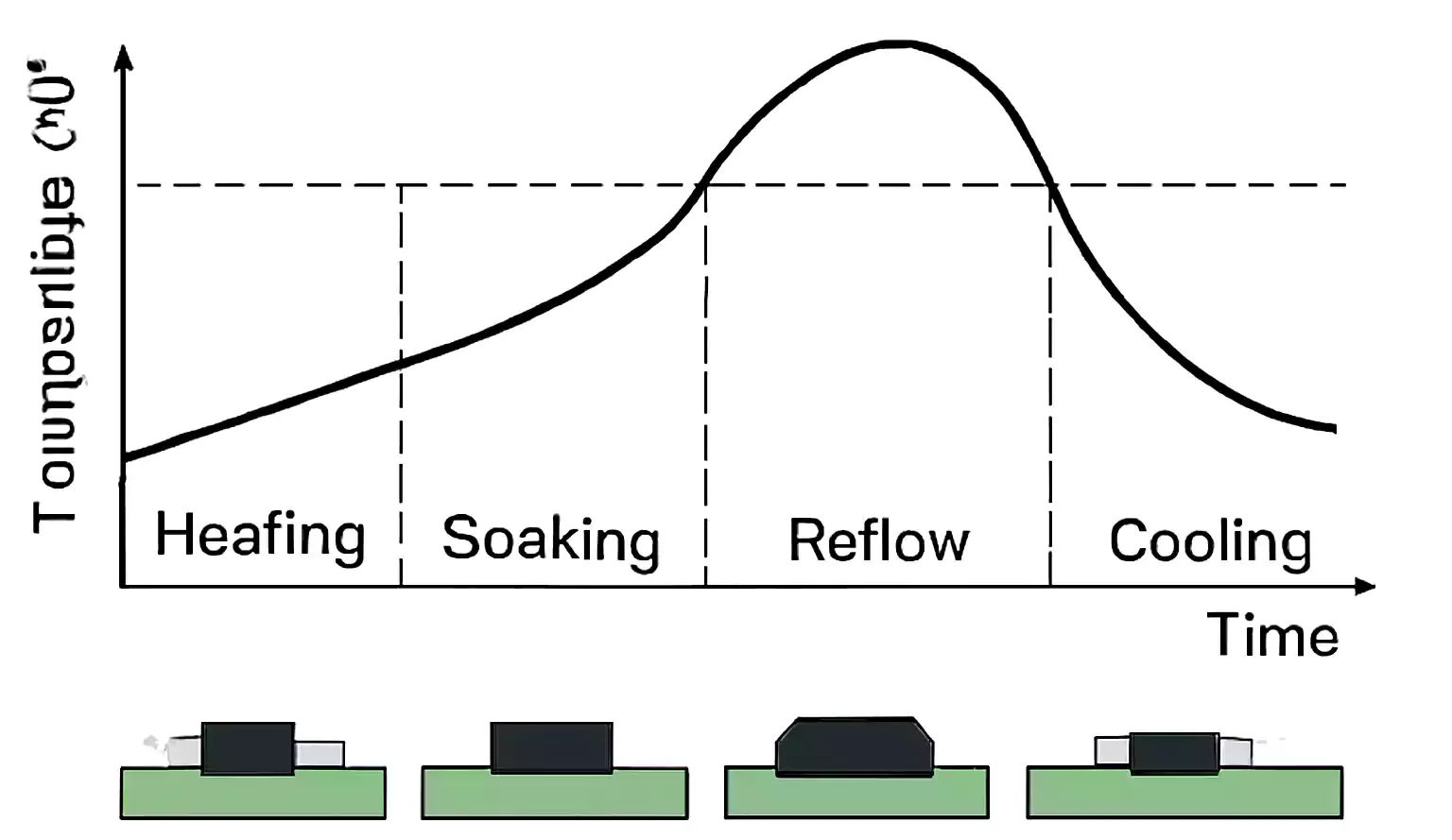
1. What Is a Reflow Profile and Why Does It Matter?
A reflow profile is a time-temperature curve used to control the heating and cooling of the solder paste and components on the PCB during reflow soldering. It determines how solder transitions from a paste into a solid, reliable electrical and mechanical connection. Proper reflow profiles ensure:
- Solder paste melts and flows correctly
- Components are not thermally damaged
- Oxidation and warping are minimized
- Solder defects are avoided
2. Key Zones of a Standard Reflow Profile
A typical SMT reflow profile consists of four main stages:
| Zone | Purpose | Typical Range |
|---|---|---|
| Preheat Zone | Gradually heats PCB and activates flux | 1.0–3.0 °C/s up to 150–180 °C |
| Soak Zone | Stabilizes temperature across PCB; removes volatiles | 60–120 seconds at 150–180 °C |
| Reflow Zone | Peak temperature melts solder | 30–60 seconds at 230–250 °C (lead-free) |
| Cooling Zone | Solidifies joints quickly to avoid grainy structures | −3.0 to −1.0 °C/s down to <100 °C |
Each stage must be tightly controlled to match the thermal mass of your PCB, the type of solder paste, and the sensitivity of components.
3. Recommended Settings for Lead-Free Reflow Soldering
Lead-free soldering is now the industry standard due to RoHS compliance. Below are typical settings for SAC305 (Tin-Silver-Copper) solder paste:
| Parameter | Recommended Value |
|---|---|
| Ramp-up Rate (Preheat) | 1.0–3.0 °C/s |
| Soak Time | 90–120 seconds |
| Soak Temperature Range | 150–180 °C |
| Time Above Liquidus (TAL) | 30–90 seconds (>217 °C) |
| Peak Reflow Temperature | 235–250 °C |
| Ramp-down Rate (Cooling) | 1.0–3.0 °C/s |
4. Recommended Settings for Leaded Reflow Soldering
For Sn63/Pb37 solder paste (used in legacy or military applications):
| Parameter | Recommended Value |
|---|---|
| Ramp-up Rate | 1.0–2.0 °C/s |
| Soak Temperature Range | 140–160 °C |
| Time Above Liquidus (TAL) | 45–75 seconds (>183 °C) |
| Peak Reflow Temperature | 210–225 °C |
| Cooling Rate | 1.0–2.0 °C/s |
5. Common Reflow Profile Defects and How to Fix Them
| Defect | Cause | Solution |
|---|---|---|
| Tombstoning | Uneven heating, small passives, wrong soak | Improve soak uniformity, adjust ramp-up |
| Cold joints | Low peak temperature or short TAL | Increase peak temp or time above liquidus |
| Solder balls | Overheated paste or rapid ramp-up | Reduce ramp rate, check stencil design |
| Voids | Volatiles not outgassed during soak | Extend soak time, optimize paste volume |
| Component damage | Excessive peak temperature | Reduce peak temp, improve thermal profiling |
6. Reflow Profile Optimization Tips
- Use a thermal profiler: Place thermocouples on actual PCB areas, including corners and dense zones
- Simulate worst-case boards: Optimize for thermal balance, especially in multilayer boards or mixed components
- Profile per product: Avoid using the same profile across product lines with different thermal properties
- Recheck profile after maintenance: Reflow ovens degrade over time; revalidate after repairs or nozzle changes
7. Advanced Profile Strategies
- Ramp-Soak-Spike (RSS): Standard for most production lines
- Ramp-to-Spike (RTS): Faster process, suited for robust assemblies
- Step-soak profiles: Used in complex boards with temperature-sensitive components
Frequently Asked Questions (FAQ) About SMT
What does SMT stand for?
SMT stands for Surface Mount Technology, a method for mounting electronic components directly onto the surface of a PCB (Printed Circuit Board).
What is the difference between SMT and THT?
SMT places components on the surface of the PCB, while THT (Through-Hole Technology) involves inserting component leads through holes in the PCB. SMT allows higher component density and automation.
What are the main steps in the SMT assembly process?
·Solder Paste Printing
·Component Placement
·Reflow Soldering
What are common defects in SMT and how can they be avoided?
Common defects:
·Solder bridging
·Tombstoning
·Misalignment
To avoid these:
·Optimize stencil design
·Use correct reflow profiles
·Regularly calibrate machines
What types of components are used in SMT?
·Passive: resistors, capacitors
·Active: ICs (SOIC, QFN, BGA)
·Others: LEDs, diodes, connectors
SMT supports high-density and precise component placement.
Is SMT suitable for high-reliability applications?
Yes, SMT is widely used in automotive, aerospace, and medical applications where high quality and reliability are crucial.
Conclusion
Surface Mount Technology (SMT) remains the industry standard for assembling high-density electronic circuits. Its ability to support compact designs, fast production cycles, and automated workflows makes it essential for today’s electronics manufacturing.
A successful SMT process depends on tight control of each production stage—solder paste printing, component placement, reflow soldering, and inspection. When managed correctly, SMT offers superior electrical performance, reduced manufacturing costs, and improved reliability.
Choosing the right equipment, optimizing reflow profiles, and minimizing defects through SPI and AOI inspection are key to maintaining consistent quality. As electronics continue to evolve toward higher complexity and miniaturization, staying current with SMT best practices is critical.