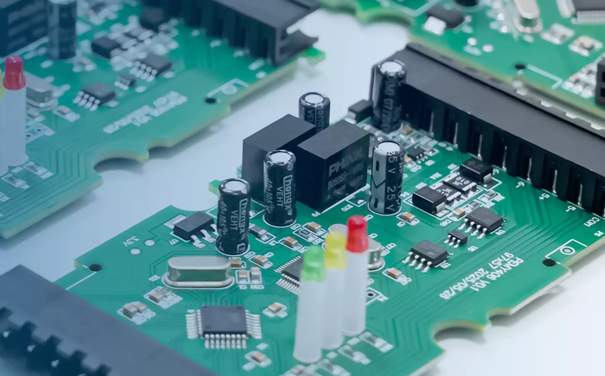
Introduction
The solder mask and silkscreen are essential layers in PCB manufacturing. The solder mask protects copper traces from oxidation and prevents solder bridging, while the silkscreen identifies component locations and orientation.
This guide covers the solder mask and silkscreen process, including how they are applied and how to design proper solder mask openings and reference markings. By following best practices, you can reduce assembly defects and improve manufacturing reliability
Solder Mask Process and Design Essentials
1.What Is Solder Mask in PCB Manufacturing?
Solder mask (also known as solder resist) is a protective layer applied to the outer surfaces of a printed circuit board (PCB). Its primary purpose is to prevent solder bridging, protect copper traces from oxidation and contamination, and enhance the board’s mechanical strength and reliability during soldering and long-term use.
Most PCBs use a green solder mask, but other colors like red, blue, black, and white are available depending on aesthetic or functional needs. The green variant is most common due to its excellent contrast during inspection and its thermal stability.
Solder mask is essential for surface-mount technology (SMT) and high-density interconnect (HDI) designs, where tight spacing between pads increases the risk of solder shorts.
2.Solder Mask Application Process: Key Manufacturing Steps
Understanding how solder mask is applied helps designers anticipate manufacturing tolerances and avoid common DFM (design for manufacturability) pitfalls.
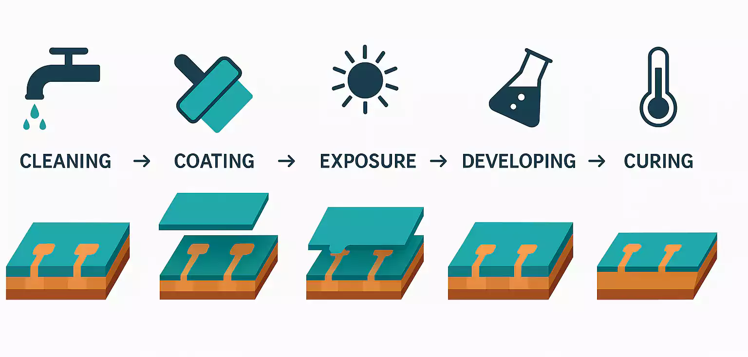
The typical solder mask process includes the following steps:
- Surface Cleaning and Preparation
The bare PCB is cleaned to remove oxidation, oil, and debris. A clean surface ensures good adhesion of the solder mask and reduces the risk of delamination. - Solder Mask Coating (Typically LPI - Liquid Photoimageable)
A thin layer of LPI solder mask is coated over the board using screen printing or curtain coating. This layer will eventually define where solder is allowed (openings) and where it’s blocked (covered areas). - Pre-baking / Tack Dry
The coated board is partially dried to remove solvents, ensuring the mask retains enough tackiness to hold its shape during the exposure process. - Exposure (Imaging)
The board is exposed to UV light through a photomask or via direct imaging (DI). Areas exposed to light harden, while unexposed areas will be removed during development. Exposure precision determines how accurately the solder mask aligns with the copper pads. - Developing
The board is sprayed with a developer solution that removes the unhardened solder mask from pad areas. Precise development ensures clean openings and prevents partial coverage over pads that could cause poor solder joints. - Final Curing (Thermal or UV)
A full cure hardens the solder mask and makes it resistant to heat, chemicals, and physical abrasion during soldering processes.
3.Solder Mask Design Guidelines and Best Practices
Even with a perfect manufacturing process, poor solder mask design can lead to defects such as solder bridging, pad coverage, or poor solderability. To ensure optimal performance, follow these key design rules:
3.1 Solder Mask Clearance / Expansion
Always expand the solder mask opening slightly beyond the copper pad to account for alignment tolerances.
- Typical recommended expansion: +3 to +5 mil (0.075 – 0.125 mm)
- Too little clearance may result in the pad being partially covered, preventing proper soldering.
3.2 Solder Mask Dam / Bridge Width
A solder dam is the area of solder mask between adjacent pads (especially in fine-pitch components like QFPs or BGA).
- Minimum recommended bridge width: 4 mil (0.1 mm), depending on manufacturer capability
- Bridges that are too narrow may break during processing, increasing the risk of solder bridging.
3.3 Solder Mask Defined (SMD) vs Non-Solder Mask Defined (NSMD) Pads
- NSMD (preferred for BGA/QFN): The solder mask opening is larger than the pad, exposing the entire pad area. This promotes better solder joint reliability and inspection visibility.
- SMD: The solder mask overlaps the pad, reducing exposed copper. Less common and usually reserved for specific mechanical constraints.
Silkscreen Process and Design Guidelines
Silkscreen, also known as the legend layer or overlay, plays a crucial role in printed circuit boards (PCBs) by providing visual identifiers for components, test points, polarity, and other critical assembly information. While silkscreen does not affect the electrical performance of a board, poor silkscreen design can impact assembly efficiency, troubleshooting, and rework accuracy.
1. What is Silkscreen in PCB?
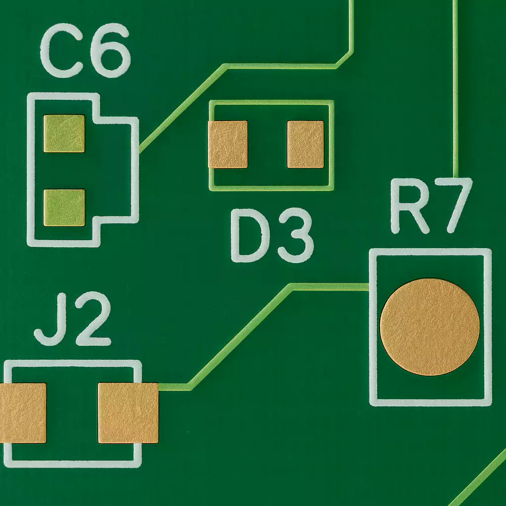
The silkscreen layer contains non-conductive ink markings printed on top of the solder mask layer. These markings typically include:
- Reference designators (e.g., R1, C3, U5)
- Polarity indicators for diodes, capacitors, LEDs
- Pin 1 markers for ICs
- Manufacturer logos, part numbers, version control
- Assembly and test labels
White ink is most commonly used for silkscreen due to its high contrast, but other colors like yellow or black may be used depending on the solder mask color.
2. Silkscreen Printing Process (Manufacturing Overview)
There are two main methods for applying silkscreen on PCBs:
- Screen Printing (Traditional)
- Uses a stencil or mesh screen to apply epoxy-based ink
- Suitable for low- to mid-volume production
- Limited resolution; cannot handle extremely fine text or dense layouts
- Direct Legend Printing (DLP or Digital Silkscreen)
- Inkjet-based method that prints text directly onto the board surface
- Offers higher resolution and better alignment with design layers
- Preferred for high-density designs and small fonts
After printing, the board is cured or baked to harden the ink and ensure durability during soldering and handling.
3. Silkscreen Design Guidelines for Reliable PCBs
To prevent issues during assembly and maintain readability, follow these silkscreen best practices:
3.1 Minimum Font Size and Line Width
- Recommended minimum font height: 1.0 mm (≈ 40 mil)
- Minimum line width: 6 mils (0.152 mm)
- Avoid overly decorative fonts—use sans-serif, vector-based fonts for clarity (e.g., Arial or OCRA)
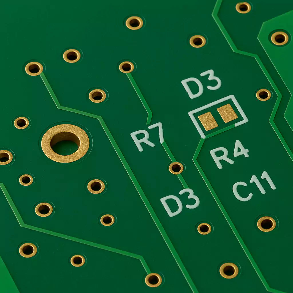
3.2 Clearance from Pads and Vias
- Maintain at least 6 mil clearance between silkscreen and:
- SMD pads
- Through-holes
- Solder mask openings
- If silkscreen ink overlaps solderable areas, it can interfere with solderability and reflow quality, leading to non-wet joints or burnt ink during soldering.
3.3 Silkscreen Placement Best Practices
- Place reference designators close to components but not under them
- Maintain consistent orientation for easy readability (e.g., all text horizontal or aligned with board edges)
- Avoid placing silkscreen in high-density BGA areas or on solder mask openings
- For two-sided boards, use silkscreen only where component visibility is possible
3.4 Avoid Overcrowding
- Don’t overload the board with redundant or unnecessary silkscreen information
- Use assembly drawings for detailed labeling if needed
3.5 Consider Assembly and Inspection
Clearly mark test points, fuse ratings, and polarities
Ensure text is large and clear enough for manual assembly and optical inspection
Common Defect Cases and Prevention Tips
Even when PCB designs pass initial checks, issues with solder mask and silkscreen can arise during manufacturing—often due to overlooked spacing, misalignment, or poor layer definitions. Below are some of the most frequent problems and how to prevent them.
1. Solder Mask Covering Pads
Issue:
Pads are partially or fully covered by solder mask, preventing proper wetting during soldering. This can cause cold joints, open circuits, or component detachment.
Root Cause:
- Inadequate solder mask expansion settings in CAD
- Misalignment during exposure or imaging
- CAM layer misinterpretation
Prevention Tips:
- Apply solder mask expansion of at least 3–5 mils beyond the copper pad edges
- Use NSMD (Non-Solder Mask Defined) pads for most SMT applications
- Review final Gerber layers to ensure clear pad openings
- Confirm alignment tolerance with your PCB fabricator
2. Solder Mask Sliver or Bridge Breakage
Issue:
Narrow solder mask slivers (or "dams") between adjacent pads can break during development or get etched away, resulting in exposed copper bridges that lead to short circuits.
Root Cause:
- Mask bridge width set below manufacturer's minimum (often <4 mils)
- Tight pitch components (e.g. QFP, BGA) without adequate solder dam design
- Over-etching during development phase
Prevention Tips:
- Maintain solder mask bridge width ≥ 4 mils (check with PCB vendor capabilities)
- Avoid "knife-edge" slivers—merge openings if bridges are too thin
- For high-density designs, communicate special requirements to fabricators
3. Silkscreen Overlapping Pads or Vias
Issue:
Silkscreen ink printed on pads or via holes can interfere with soldering, causing unreliable connections, burn marks, or contamination during reflow.
Root Cause:
- No clearance rule between silkscreen and copper layers
- Manual label placement too close to SMD pads
- Lack of silkscreen DRC in design software
Prevention Tips:
- Maintain a minimum clearance of 5 mils between silkscreen and pads
- Use design rule checks (DRC) to catch silkscreen–pad overlap
- Avoid placing reference designators inside BGA areas or over test points
- In critical zones, consider suppressing silkscreen altogether
4. Incomplete or Residual Solder Mask
Issue:
After development, some areas retain partially developed solder mask, leading to contamination, poor solderability, or inconsistent visual inspection.
Root Cause:
- Underexposure or insufficient development time
- Contaminated board surface prior to coating
- Thick or uneven solder mask application
Prevention Tips:
- Ensure proper pre-cleaning and surface prep before mask coating
- Use validated exposure/development profiles with your vendor
- Conduct AOI or visual checks after mask development to spot residual
New Technologies and Trends in Solder Mask and Silkscreen
As PCB designs become denser and more complex, the technologies used for solder mask and silkscreen application are evolving rapidly to meet modern manufacturing demands.
1. Inkjet-Printed Solder Mask
Traditional photoimageable solder masks (LPI) require multiple steps, including coating, imaging, and development. However, inkjet solder mask printing is gaining traction as a high-precision, direct-write alternative. It eliminates the need for phototools, reduces alignment errors, and minimizes material waste. This technique is particularly useful for HDI boards and prototypes requiring faster turnaround.
2. Digital Silkscreen Printing
Conventional silkscreen methods struggle with fine pitch components and small designators. Digital silkscreen printing, using inkjet or UV laser technologies, offers higher resolution and better alignment. It allows for smaller fonts, precise positioning, and improved durability, especially important in compact or high-reliability PCBs.
3. Material Advancements
New solder mask materials with enhanced thermal stability, low dielectric loss, and RoHS-compliant, halogen-free compositions are becoming standard for high-speed and high-temperature applications. These advanced materials improve PCB reliability under reflow soldering and lead-free processing conditions.
Frequently Asked Questions (FAQ)
Can solder mask cover pads or vias?
No. Solder mask should not cover pads unless via tenting is intended. Covering pads may cause poor solderability or open joints.
What is the ideal solder mask expansion?
Typically 3–5 mils beyond the copper pad. This allows for alignment tolerance and ensures the pad is fully exposed.
What’s the minimum readable silkscreen text size?
At least 1 mm height with 6 mil line width is recommended for clarity after soldering.
Can silkscreen overlap solderable areas?
No. Keep at least 5 mil clearance from pads or vias to avoid soldering issues.
What’s the difference between SMD and NSMD pads?
·SMD: Solder mask overlaps pad edges.
·NSMD: Pad is fully exposed. Preferred for most SMT designs.
Conclusion
The solder mask and silkscreen layers are essential for PCB reliability and manufacturability. A properly applied solder mask prevents solder bridging, protects copper surfaces, and enhances electrical insulation. The silkscreen layer, on the other hand, ensures accurate component placement and clear identification during assembly and inspection.
By following correct design practices—such as proper solder mask expansion, clearance, and silkscreen alignment—you can avoid common production issues like pad coverage or misregistration. Careful attention to these details during the design stage not only improves solderability but also reduces defects and rework.
Want to ensure your next PCB design passes DFM checks smoothly? Start by mastering the solder mask and silkscreen process.