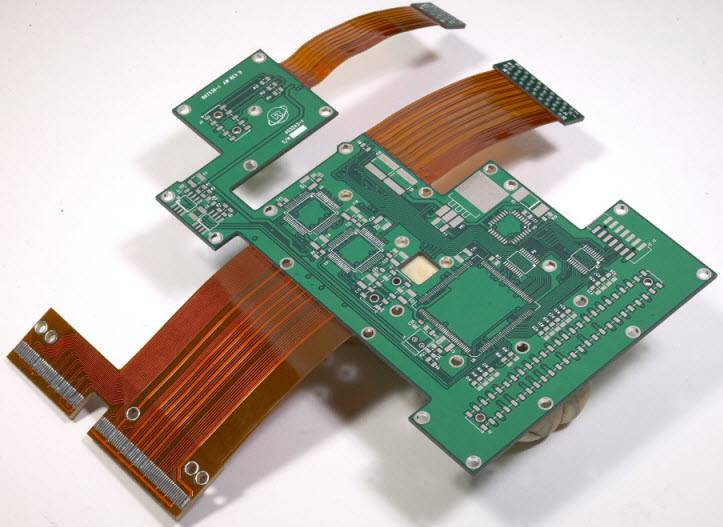
Introduction
Prototyping a PCB is a critical step in hardware development. But when you're assembling just a few boards, traditional assembly services can be costly, slow, or have high minimum order requirements.
This is where manual tools and low-volume assembly techniques make a difference. For hardware engineers and hand-soldering professionals, mastering these methods enables faster iterations, lower costs, and better control during early-stage testing.
In this guide, we’ll cover practical techniques for prototype PCB assembly, from paste application and component placement to reflow, inspection, and rework. You'll also find tool recommendations and workflow tips designed to streamline small-batch production.
Prototype PCB Assembly Process Overview
When working on hardware prototypes, time, cost, and flexibility are critical. Whether you're assembling one board by hand or producing a low-volume batch in a lab, understanding the full prototype PCB assembly process helps ensure a smoother build and faster design validation.
Here’s a high-level overview of the standard prototype PCB assembly workflow:
1. Design Finalization & DFM Check
Before any physical assembly, ensure your PCB layout passes basic Design for Manufacturability (DFM) checks. This includes correct pad sizing, solder mask clearance, component spacing, and routing. A well-prepared design can significantly reduce rework during assembly.
2. Bill of Materials (BOM) Preparation
A clean, well-organized BOM is crucial. It should include exact part numbers, preferred footprints, quantities, and potential alternates—especially important for sourcing in small volumes.
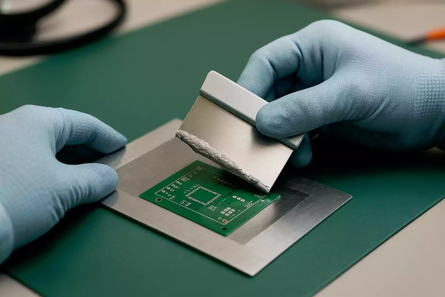
3. Stencil or Solder Paste Application
Depending on your method, you may use a stencil (laser-cut or framed) to apply solder paste or manually dispense it with a syringe. For fine-pitch components, a stencil ensures consistent results.
4. Component Placement
This step can be fully manual (with tweezers), semi-automated (using a desktop pick-and-place machine), or outsourced. Proper orientation, alignment, and gentle placement are essential—especially for small passive components or ICs.
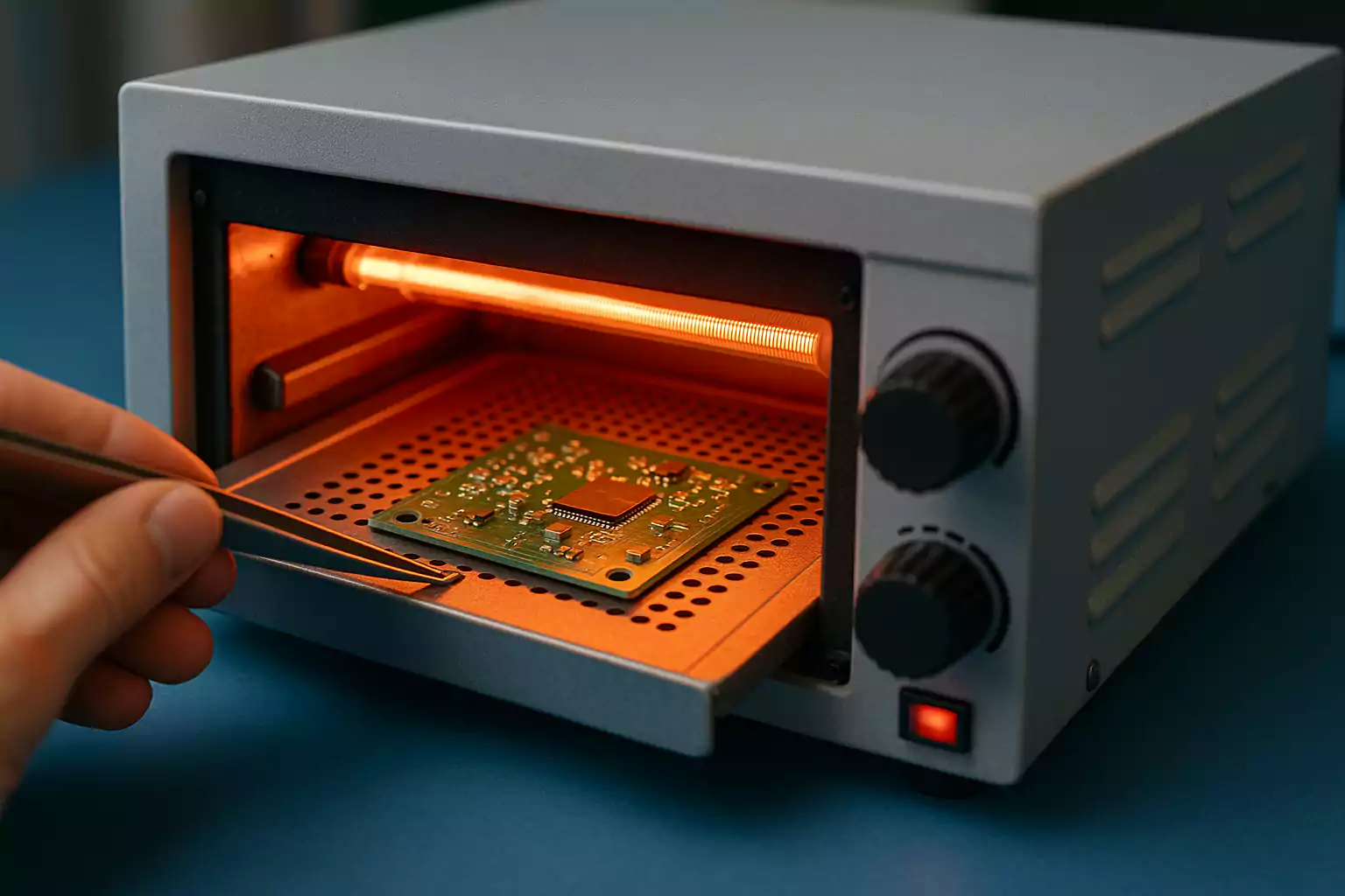
5. Reflow Soldering or Manual Soldering
If using solder paste, you'll need a reflow oven or a controlled hot-air station to melt the paste and secure the components. For through-hole parts or specific components, manual soldering may still be required.
6. Inspection and Testing
After assembly, conduct a thorough inspection for solder bridges, cold joints, misalignments, or tombstoning. Use visual magnification or low-cost microscopes. Basic continuity and power-up tests help catch early functional issues.
7. Rework (if needed)
Prototype boards often require one or more rework cycles. Hot air tools, solder wick, and flux are standard tools for making clean adjustments or fixing assembly issues.
8. Firmware/Software Upload and Validation
Once the board is physically complete, proceed with firmware flashing and early functional tests. This stage confirms that both your design and assembly were successful.
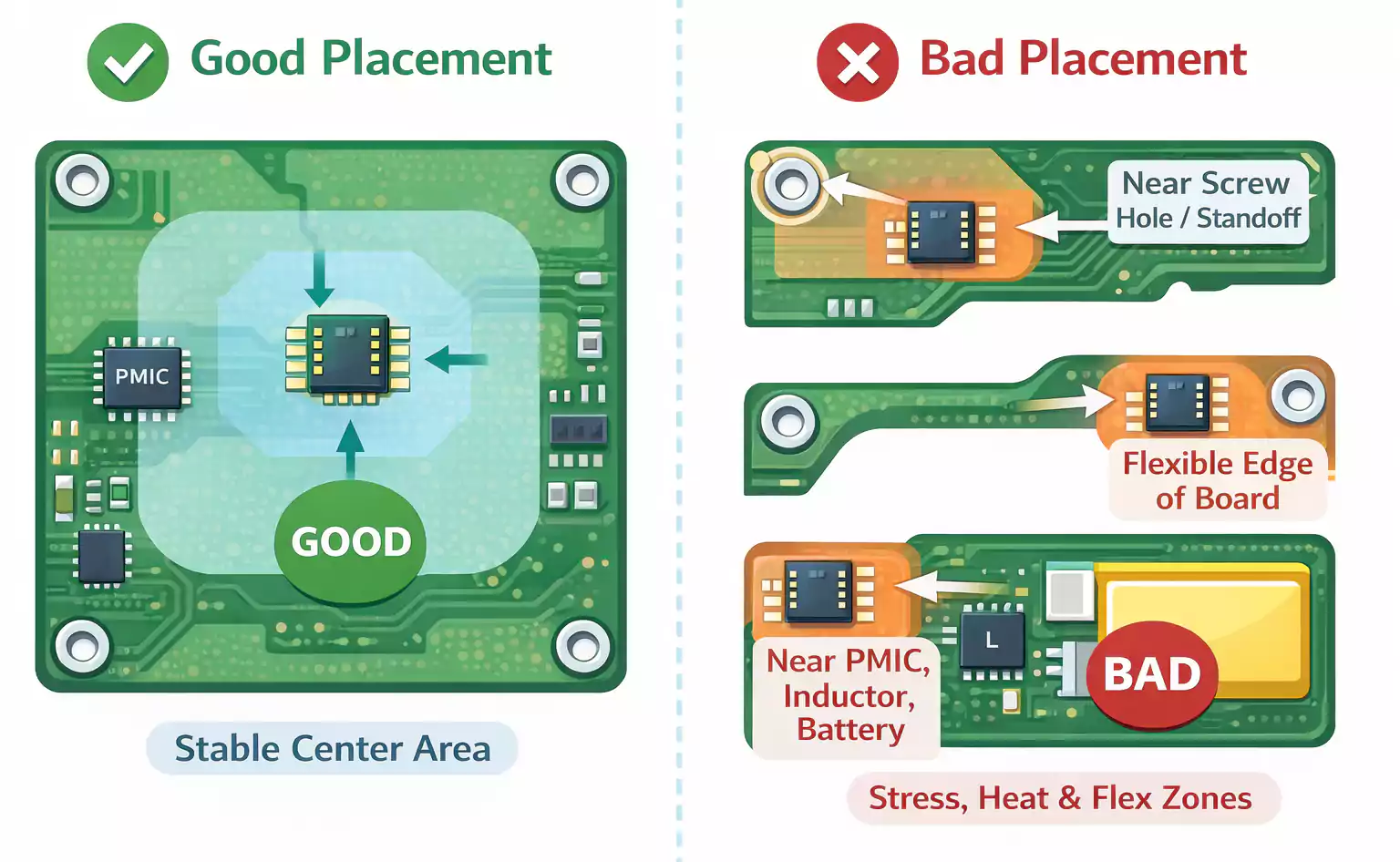
Design and DFM Preparation for Prototypes
Effective prototype PCB assembly starts with a design optimized for manufacturability—especially when you're working with low-volume or manual tools.
Key DFM Guidelines for Prototyping
- Use Standard Packages
Stick to 0603, 0805, SOIC, and SOT-23 where possible. Avoid fine-pitch BGAs or 01005 unless necessary. - Increase Pad Size and Spacing
Slightly enlarged pads and wider spacing simplify manual soldering and reduce bridging risks. - Avoid Vias in Pads
Use via tenting or fill techniques to prevent solder wicking. - Align Component Orientation
Keep polarized parts and ICs facing the same direction to reduce placement errors. - Add Fiducials and Clear Silkscreen
Include fiducials for alignment and ensure all markings are visible and readable. - Expose Test Points
Make sure key nets are accessible for probing during testing and bring-up. - Use Thermal Reliefs
Avoid solid plane connections to pads—use thermal reliefs to ease soldering.
Prototype-Friendly Design Adjustments
- Use larger components when possible.
- Prioritize visibility and testability over density.
- Avoid complex stack-ups unless required.
BOM Strategy and Sourcing Tips
Creating a streamlined Bill of Materials (BOM) is essential for successful prototype PCB assembly—especially when working with manual tools or low-volume builds.
1. Choose Common, In-Stock Components
Use standard footprints and values that are widely available from distributors like Digi-Key, Mouser, or LCSC. For manual soldering, 0603 or 0805 passives and SOIC or TQFP ICs are ideal. Avoid rare or obsolete parts.
2. Add Backup Part Numbers
Always include substitutes for key components. Adding an “Alternative Part” column in your BOM helps avoid delays due to stock issues or lead times.
3. Order Extra Components
Account for handling loss or soldering mistakes:
- Passives: 2–3× needed quantity
- ICs/Connectors: Add 10–20% buffer
4. Use Prototype-Friendly Packaging
For manual assembly, prefer loose parts or short cut tape. Avoid full reels unless using pick-and-place machines. Watch out for high shipping costs on small orders.
5. Keep the BOM Lean
Start with the essentials. A minimal BOM allows for quicker iteration and easier troubleshooting during the prototype phase
Assembly Methods Comparison & Selection Guide
When working on prototype PCB assembly, choosing the right assembly approach depends on your batch size, budget, and equipment availability. The table below summarizes the most common options used by engineers and makers for low‑volume and manual assembly.
| Assembly Method | Best For | Typical Quantity | Key Advantages | Main Limitations | Recommended Tools / Setup |
|---|---|---|---|---|---|
| Manual Hand Soldering | R&D engineers, repair, and quick one‑off prototypes | 1–5 pcs | • Lowest cost setup • No stencil required • Full control for rework | • Time‑consuming • Inconsistent solder joints • Difficult for fine‑pitch parts | Soldering iron (Hakko/Weller), flux pen, tweezers, magnifier, hot‑air rework station |
| Manual Solder Paste + Reflow | Functional boards with mixed SMD components | 1–20 pcs | • Consistent results • Handles small SMD packages • Similar to production process | • Requires stencil • Risk of misalignment without pick‑and‑place aid | Solder paste, stencil, scraper, desktop reflow oven (T‑962 / Puhui), IR thermometer |
| Desktop Pick‑and‑Place + Reflow | Engineering teams or labs producing small batches | 5–100 pcs | • Fast placement for multiple boards • Higher accuracy • Lower labor cost over time | • Higher initial equipment cost • Setup requires calibration | Desktop pick‑and‑place (Neoden, Charmhigh), reflow oven, air compressor, vision alignment |
| Outsourced Quick‑Turn PCB Assembly | When in‑house labor or tools are unavailable | 10–200 pcs | • Fast turnaround (1–3 days typical) • Professional reflow and AOI testing • Saves engineering time | • Higher per‑unit cost for small runs • Limited design iteration flexibility | Turnkey assembly service (ProtoExpress, PCBWay, JLCPCB, MacroFab) |
Selection Tips
- 1–5 pcs: Use manual soldering for quick functional tests or early validation.
- 5–20 pcs: Choose manual solder paste + reflow to improve repeatability.
- 20–100 pcs: Desktop automation (pick‑and‑place + reflow) provides better speed and consistency.
- 100+ pcs or tight deadlines: Outsource to a quick‑turn PCB assembly service for professional quality and faster turnaround.
Core Assembly Techniques: Solder Paste, Component Placement, and Reflow
Effective prototype PCB assembly depends on getting three core steps right: solder paste application, component placement, and reflow soldering. This section shares streamlined techniques optimized for manual work and low-volume runs.
1. Solder Paste Application (Manual Stenciling)
- Use laser-cut stainless-steel stencils for consistency; frameless versions are cost-effective for prototyping.
- Fix the PCB on a flat surface; apply paste with a 45° squeegee angle using even pressure.
- Avoid re-sweeping—one smooth pass is ideal to prevent smearing or uneven deposition.
- Inspect under magnification: paste should fully cover each pad with clean edges.
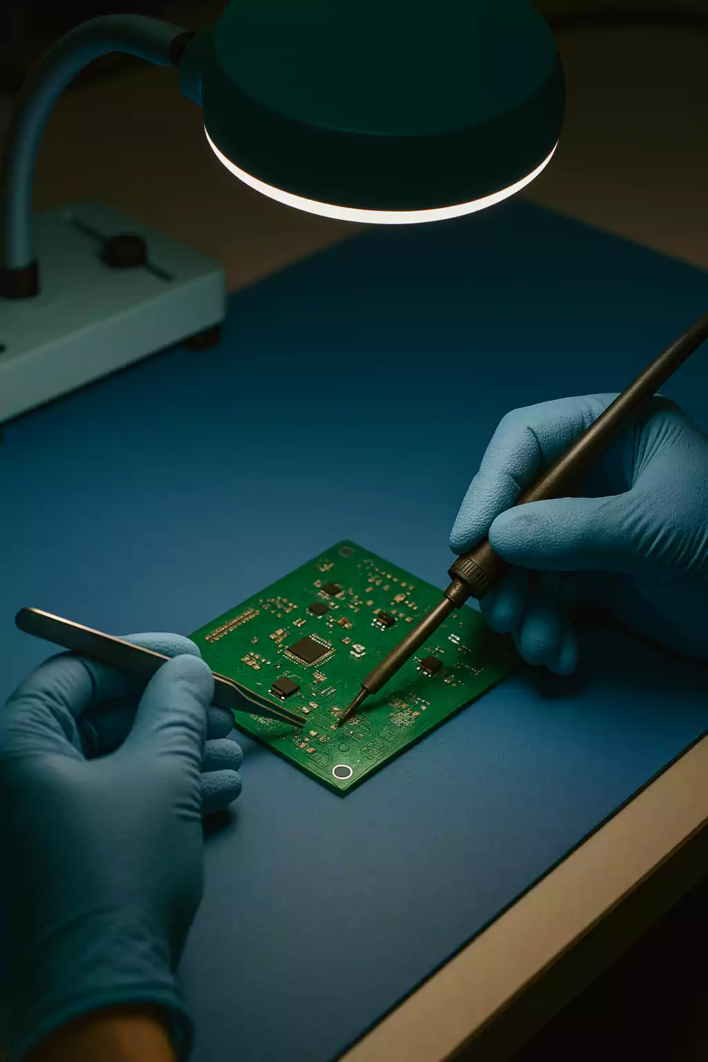
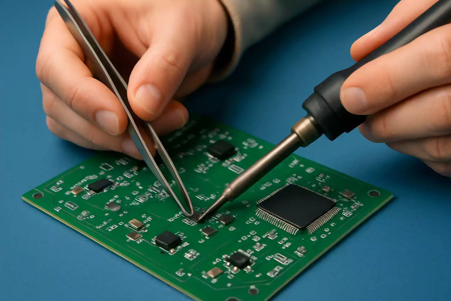
2. Component Placement (Tweezers or PnP)
- Use fine-point, ESD-safe tweezers for manual work; handle parts by the body to avoid lead damage.
- Let the solder paste hold the part—don’t press hard.
- Start with smallest components first, then move to large ones.
- Double-check polarity of diodes, ICs, and electrolytic capacitors.
3. Reflow Soldering (Oven or Hot Air)
Option A: Desktop Reflow Oven (Recommended)
- Follow paste manufacturer’s reflow profile. Typical lead-free curve:
- Preheat: 150–180°C
- Soak: 180–200°C
- Peak: 230–245°C
- Cool: gradual, room temp
- Use thermal probes to validate heat zones.
Option B: Hot Air Station (1–3 boards only)
- Move nozzle in circles, ~1–2 cm above parts.
- Watch for solder flow and part alignment.
- Avoid overheating, especially on ICs.
Common Issues & Fixe
| Problem | Likely Cause | Fix |
|---|---|---|
| Solder bridges | Excess paste | Use thinner stencil / less paste |
| Tombstoning | Uneven heating | Improve pad symmetry & heating |
| Cold joints | Low reflow temp | Verify oven profile |
| Part shift | Weak paste hold | Improve placement precision |
Inspection, Testing, and Rework
Once your prototype PCB assembly is complete, a thorough inspection and testing phase is critical to ensure functionality and reduce downstream failures.
Visual Inspection: First Line of Defense
Begin with a visual inspection under magnification (≥5x) or a digital microscope. Focus on:
- Solder joints: Look for cold joints, cracks, or incomplete wetting.
- Component alignment: Ensure leads are centered on pads, especially for fine-pitch ICs.
- Solder bridges: Common between pins of QFP, SOIC, and 0402 passives.
A simple checklist for visual inspection can dramatically reduce error rates in hand or low-volume assemblies.
Functional Testing Basics
Use a multimeter to perform:
- Continuity testing: Verify key power, ground, and signal lines.
- Short circuit detection: Across power rails and between adjacent pins.
If your board includes firmware or programmable components, use a basic smoke test before loading software. For high-reliability designs, consider boundary scan or test jigs.
Common Rework Procedures
Rework is inevitable in prototype assembly. Here’s how to handle it effectively:
- Hot air rework stations help remove and replace SMT components without damaging pads.
- Desoldering braid or vacuum pumps aid in solder cleanup.
- Always clean with IPA after rework to remove flux residues.
Maintaining proper temperature profiles during rework prevents pad lifting or delamination.
Conclusion
Prototype PCB assembly plays a vital role in fast, cost-effective hardware development. By applying proper DFM principles, choosing the right tools, and using low-volume soldering techniques, engineers and makers can quickly validate designs without relying on full-scale production.
This guide outlined practical steps—from manual assembly methods to troubleshooting tips—to help you build high-quality PCB prototypes in-house. With the right workflow and preparation, even small teams can achieve professional results.
Ready to get started? Download our free DFM checklist and tool guide to streamline your next build